DM9008 Ver la hoja de datos (PDF) - Davicom Semiconductor, Inc.
Número de pieza
componentes Descripción
Lista de partido
DM9008 Datasheet PDF : 68 Pages
| |||
Absolute Maximum Ratings*
Supply Voltage (VCC) . . . . . . . . . . . . . . . . -0.5V to +7.0V
DC Input Voltage (Vin) . . . . . . . . . . . -0.5V to VCC +0.5V
DC Output Voltage (Vout) . . . . . . . . . -0.5V to VCC +0.5V
Storage Temperature Range (Tstg) . . . -65°C to + 150°C
Power Dissipation (PD) . . . . . . . . . . . . . . . . . . . . 500 mW
Lead Temp. (TL) (Soldering, 10 sec.) . . . . . . . . . . 220°C
Ambient Temperature Range (TA)……………0°C to 70°C
Case Temp. (Tc) . . . . . . . . . . . . . . . . . . . . . . 0°C to 85°C
ESD rating (Rzap = 1.5k, Czap = 120 pF) . . . . . . . 4000V
Differential Input Voltage . . . . . . . . . . . . . . . -5.5V to 16V
Differential Output Voltage . . . . . . . . . . . . . . . . 0V to 16V
DM9008
ISA/Plug & Play Super Ethernet Contoller
*Comments
Stresses above those listed under "Absolute Maximum
Ratings" may cause permanent damage to this device. These
are stress ratings only. Functional operation of this device at
these or any other conditions above those indicated in the
operational sections of this specification is not implied or
intended. Exposure to the absolute maximum rating conditions
for extended periods may affect device reliability.
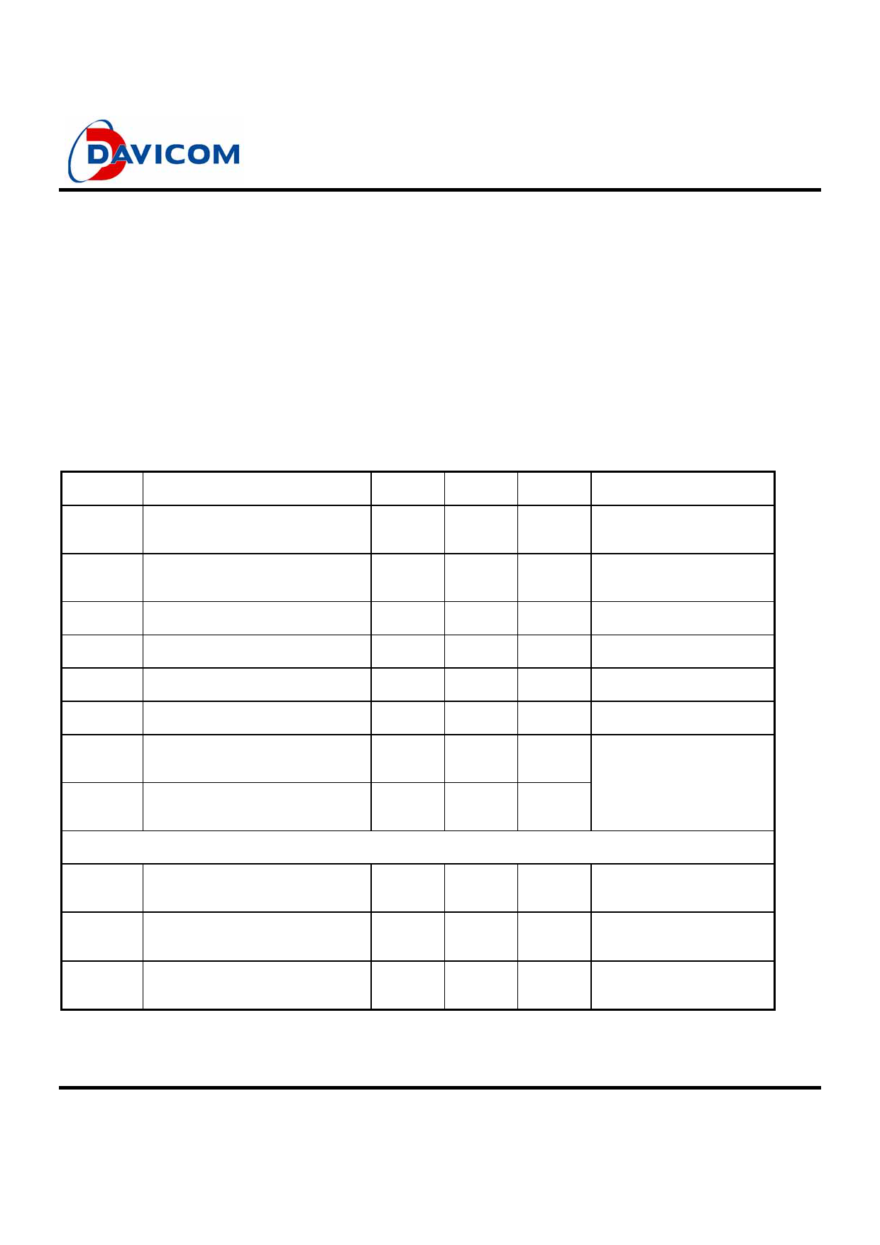
DC Electrical Characteristics (VCC = 5V ± 5%, TA = 25°C, unless otherwise specified)
Symbol
Parameter
Min.
Max.
Unit
Conditions
Voh
High Level Output Voltage
(Notes 1, 2)
VCC - 0.1
3.5
V
Ioh = -20 A
V
Ioh = -2.0mA
Vol
Low Level Output Voltage
(Notes 1, 2)
0.1
V
Iol = 20 A
0.4
V
Iol = 2.0mA
Vih
High Level Input Voltage (Note 6)
3.0
V
Vil
Low Level Input Voltage (Note 6)
0.8
V
Iin
Input Current
-1.0
+1.0
A
Vi = VCC or GND
Ioz
Tri-state Output Leakage Current
-10
+10
A
Vout = VCC or GND
Icco
Operating VCC + AVCC Supply
Current (Note 3)
Iccs
Standby VCC + AVCC Supply
Current (Note 4)
120
mA
X1 = 20 Mhz
Iout = 0 A
110
mA
Vin = VCC or GND
Differential Pins (TX+/TX-, RX+/RX-, CD+/CD)
VOD
Differential Output Voltage (TX±)
+550
+1200
mV
78 ohm termination and
270 ohms from each to GND
VOB
Differential Output Voltage
Imbalance (TX±)
40
mV
78 ohm termination and
270 ohms from each to GND
VU
Undershoot Voltage (TX±)
100
mV
78 ohm termination and
270 ohms from each to GND
Final
3
Version: DM9008-DS-F02
November 30, 2000
Share Link: 