CS5531-AS Ver la hoja de datos (PDF) - Cirrus Logic
Número de pieza
componentes Descripción
Lista de partido
CS5531-AS Datasheet PDF : 50 Pages
| |||
CS5531/32/33/34-AS
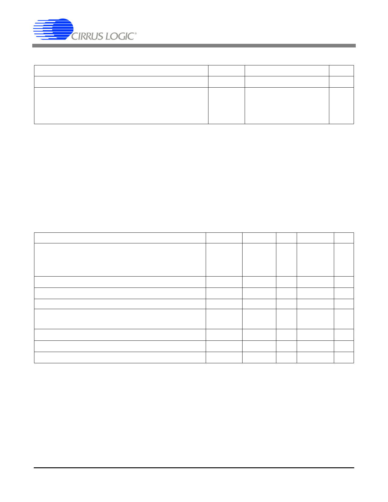
DYNAMIC CHARACTERISTICS
Parameter
Symbol
Ratio
Unit
Modulator Sampling Rate
fs
Filter Settling Time to 1/2 LSB (Full-scale Step Input)
Single Conversion mode (Notes 17, 18, and 19)
ts
Continuous Conversion mode, OWR < 3200 Sps
ts
Continuous Conversion mode, OWR ≥ 3200 Sps
ts
MCLK/16
Sps
1/OWRSC
s
5/OWRsinc5 + 3/OWR
s
5/OWR
s
17. The ADCs use a Sinc5 filter for the 3200 Sps and 3840 Sps output word rate (OWR) and a Sinc5 filter
followed by a Sinc3 filter for the
(FRS = 0) word rate associated
owtihtherthOeWSRinsc.5OfiWlteRr.sinc5
refers
to
the
3200
Sps
(FRS
=
1)
or
3840
Sps
18. The single conversion mode only outputs fully settled conversions. See Table 1 for more details about
single conversion mode timing. OWRSC is used here to designate the different conversion time
associated with single conversions.
19. The continuous conversion mode outputs every conversion. This means that the filter’s settling time
with a full-scale step input in the continuous conversion mode is dictated by the OWR.
ABSOLUTE MAXIMUM RATINGS
(DGND = 0 V; See Note 20.)
DC Power Supplies
Parameter
Input Current, Any Pin Except Supplies
Output Current
Power Dissipation
Analog Input Voltage
Digital Input Voltage
Ambient Operating Temperature
Storage Temperature
(Notes 21 and 22)
Positive Digital
Positive Analog
Negative Analog
(Notes 23 and 24)
(Note 25)
VREF pins
AIN Pins
Symbol
VD+
VA+
VA-
IIN
IOUT
PDN
VINR
VINA
VIND
TA
Tstg
Min
Typ
Max Unit
-0.3
-
+6.0
V
-0.3
-
+6.0
V
+0.3
-
-3.75
V
-
-
±10
mA
-
-
±25
mA
-
-
500
mW
(VA-) -0.3 - (VA+) + 0.3 V
(VA-) -0.3 - (VA+) + 0.3 V
-0.3
- (VD+) + 0.3 V
-40
-
85
°C
-65
-
150
°C
Notes: 20. All voltages with respect to ground.
21. VA+ and VA- must satisfy {(VA+) - (VA-)} ≤ +6.6 V.
22. VD+ and VA- must satisfy {(VD+) - (VA-)} ≤ +7.5 V.
23. Applies to all pins including continuous overvoltage conditions at the analog input (AIN) pins.
24. Transient current of up to 100 mA will not cause SCR latch-up. Maximum input current for a power
supply pin is ±50 mA.
25. Total power dissipation, including all input currents and output currents.
WARNING: Operation at or beyond these limits may result in permanent damage to the device.
Normal operation is not guaranteed at these extremes.
DS289F5
9
Share Link: 