PFS726 Ver la hoja de datos (PDF) - Power Integrations, Inc
Número de pieza
componentes Descripción
Lista de partido
PFS726 Datasheet PDF : 30 Pages
| |||
PFS704-729EG
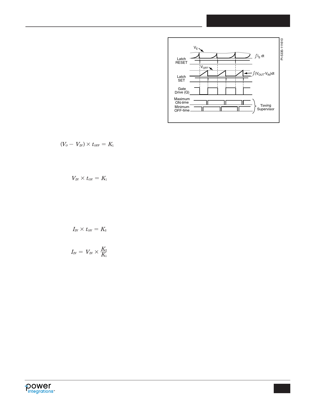
Functional Description
The HiperPFS is a variable switching frequency boost PFC
solution. More specifically, it employs a constant amp-second
on-time and constant volt-second off-time control algorithm.
This algorithm is used to regulate the output voltage and shape
the input current to comply with regulatory harmonic current
limits (high power factor). Integrating the switch current and
controlling it to have a constant amp-sec product over the
on-time of the switch allows the average input current to follow
the input voltage. Integrating the difference between the output
and input voltage maintains a constant volt-second balance
dictated by the electro-magnetic properties of the boost inductor
and thus regulates the output voltage and power.
VE
Latch
RESET
Latch
SET
Gate
Drive (Q)
Maximum
ON-time
Minimum
OFF-time
VOFF
IS dt
(VOUT-VIN)dt
Timing
Supervisor
More specifically, the control technique sets constant volt-
seconds for the off-time (tOFF). The off-time is controlled such
that:
(1)
Since the volt-seconds during the on-time must equal the
volt-seconds during the off-time, to maintain flux equilibrium in
the PFC choke, the on-time (tON) is controlled such that:
(2)
The controller also sets a constant value of charge during each
on-cycle of the power MOSFET. The charge per cycle is varied
gradually over many switching cycles in response to load
changes so it can be regarded as substantially constant for a
half line cycle. With this constant charge (or amp-second)
control, the following relationship is therefore also true:
(3)
Substituting tON from (2) into (3) gives:
(4)
The relationship of (4) demonstrates that by controlling a constant
amp-second on-time and constant volt-second off-time, the input
current IIN is proportional to the input voltage VIN, therefore
providing the fundamental requirement of power factor correction.
Figure 4. Idealized Converter Waveforms.
cycle on-time. Internally the difference between the input and
output voltage is derived and the resultant is scaled, integrated,
and compared to a voltage reference (VOFF) to determine the
cycle off-time. Careful selection of the internal scaling factors
produce input current waveforms with very low distortion and
high power factor.
The input voltage is internally synthesized using the switch duty
cycle and a 7 kHz low pass filter. This synthesized input voltage
representation is subtracted from a fixed reference voltage (6 V)
to derive a current source proportional to (VO-VIN). Please refer to
Figure 3.
Line Feed-Forward Scaling Factor (MON)
The VOLTAGE MONITOR (V) pin current is used internally to
derive the peak of the input line voltage which is used to scale
the gain of the current sense signal through the MON variable.
This contribution is required to reduce the dynamic range of the
control feedback signal as well maintain a constant loop gain
over the operating input line range. This line-sense feed-
forward gain adjustment is proportional to the square of the
peak rectified AC line voltage and is adjusted as a function of V
pin current. The line-sense feed-forward gain is also important
in providing a switch power limit over the input line range.
Besides modifying brown- in/out thresholds, the V pin resistor
also affects power limit of the device
This control produces a continuous mode power switch current
waveform that varies both in frequency and peak current value
across a line half-cycle to produce an input current proportional
to the input voltage.
Control Engine
The controller features a low bandwidth error-amplifier which
connects its non-inverting terminal to an internal voltage
reference of 6 V. The inverting terminal of the error-amplifier is
available on the external FEEDBACK pin which connects to the
external feedback resistor divider, transient load speed-up and
compensation networks to regulate the output voltage.
The internal sense-FET switch current is integrated and scaled
by the input voltage peak detector current sense gain (MON) and
compared with the error-amplifier signal (VE) to determine the
www.power.com
This characteristic is optimized to maintain a relatively constant
internal error-voltage level at full load from an input line of 100
to 230 VAC input (PFS704-716).
Beyond the specified peak power rating of the device, the
internal power limit feature will regulate the output voltage
below the set regulation threshold as a function of output
overload beyond the peak power rating. Figure 5 illustrates the
typical regulation characteristic as function of load.
Soft-Start with Pin-to-Pin Short-Circuit Protection
Since the FEEDBACK pin is the interface for output voltage
regulation (resistor voltage divider to output voltage) as well as
loop compensation (series RC), the typical application circuit of
the HiperPFS requires an external transistor network to overcome
the inherently slow feedback loop response. Specifically, an
5
Rev. G 06/15
Share Link: 