82077AA-1 Ver la hoja de datos (PDF) - Intel
Número de pieza
componentes Descripción
Lista de partido
82077AA-1 Datasheet PDF : 62 Pages
| |||
82077AA
The tuning of the PLL for tape characteristics can
also be done in hardware If a 0 (GND) is applied to
pin 39 (PLL0) the PLL is optimized for tape drives a
1 (VCC) optimizes the PLL for floppies This hard-
ware selection mechanism overrides the software
selection scheme A typical hardware application
would route the Drive Select pin used for tape drive
support to pin 39 (PLL0)
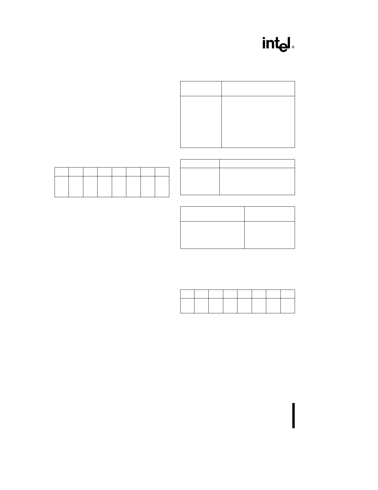
2 1 5 DATARATE SELECT REGISTER (DSR)
This register is included for compatibility with the
82072 floppy controller and is write-only Changing
the data rate changes the timings of the drive con-
trol signals To ensure that drive timings are not vio-
lated when changing data rates choose a drive tim-
ing such that the fastest data rate will not violate the
timing
7
6
5
S W POWER
0
RESET DOWN
4
3
2
1
0
PRE-
COMP
2
PRE-
COMP
1
PRE-
DRATE DRATE
COMP
SEL 1 SEL 0
0
This register is the same as used in the 82072 ex-
cept that the internal external PLL select bit is re-
moved It is recommended that bit 5 be written with
a 0 for compatibility
S W RESET behaves the same as DOR RESET ex-
cept that this reset is self clearing
POWER DOWN deactivates the internal clocks and
shuts off the oscillator Disk control pins are put in
an inactive state All input signals must be held in a
valid state (D C level 1 or 0) POWER DOWN is exit-
ed by activating one of the reset functions
PRECOMP 0–2 adjusts the WRDATA output to the
disk to compensate for magnetic media phenomena
known as bit shifting The data patterns that are sus-
ceptible to bit shifting are well understood and the
82077AA compensates the data pattern as it is writ-
ten to the disk The amount of precompensation is
dependent upon the drive and media but in most
cases the default value is acceptable
The 82077AA starts precompensating the data pat-
tern starting on Track 0 The CONFIGURE com-
mand can change the track that precompensating
starts on Table 2-2 lists the precompensation val-
ues that can be selected and Table 2-3 lists the de-
fault precompensation values The default value is
selected if the three bits are zeros
DRATE 0–1 select one of the four data rates as
listed in Table 2-4 The default value is 250 Kbps
upon a chip (‘‘Hardware’’) reset Other (‘‘Software’’)
Resets do not affect the DRATE or PRECOMP bits
Table 2-2 Precompensation Delays
PRECOMP
432
Precompensation Delay
111
0 00 ns DISABLED
001
41 67 ns
010
83 34 ns
011
125 00 ns
100
166 67 ns
101
208 33 ns
110
250 00 ns
000
DEFAULT
Table 2-3 Default Precompensation Delays
Data Rate
Precompensation Delays
1 Mbps
500 Kbps
300 Kbps
250 Kbps
41 67 ns
125 ns
125 ns
125 ns
Table 2-4 Data Rates
DRATESEL
1
0
DATA RATE
MFM
1
1
1 Mbps
0
0
500 Kbps
0
1
300 Kbps
1
0
250 Kbps
2 1 6 MAIN STATUS REGISTER (MSR)
The Main Status Register is a read-only register and
is used for controlling command input and result out-
put for all commands
7
6
5
4
3
2
1
0
NON CMD DRV 3 DRV 2 DRV 1 DRV 0
RQM DIO
DMA BSY BUSY BUSY BUSY BUSY
RQM Indicates that the host can transfer data if
set to a 1 No access is permitted if set to a 0
DIO Indicates the direction of a data transfer once
RQM is set A 1 indicates a read and a 0 indicates a
write is required
NON-DMA This mode is selected in the SPECIFY
command and will be set to a 1 during the execution
phase of a command This is for polled data trans-
fers and helps differentiate between the data trans-
fer phase and the reading of result bytes
10
Share Link: 