82077AA-1 Ver la hoja de datos (PDF) - Intel
Número de pieza
componentes Descripción
Lista de partido
82077AA-1 Datasheet PDF : 62 Pages
| |||
82077AA
monitors the status of the DMA Request pin The
STEP bit is latched with the Step output going active
and is cleared with a read to the DIR register Hard-
ware or Software RESET
2 1 2a STATUS REGISTER B (SRB PS 2 MODE)
This register is read-only and monitors the state of
several disk interface pins This register is part of the
PS 2 register set and is not accessible in PC-AT
mode
76
5
4
3
2
1
0
DRIVE WRDATA RDDATA
MOT MOT
11
WE
SEL 0 TOGGLE TOGGLE
EN1 EN0
As the only drive input RDDATA TOGGLE’s activity
is independent of the INVERT pin level and reflects
the level as seen on the cable
The two TOGGLE bits do not read back the state of
their respective pins directly Instead the pins drive
a Flip Flop which produces a wider and more reli-
ably read pulse Bits 6 and 7 are undefined and al-
ways return a 1
After any reset the activity on the TOGGLE pins are
cleared Drive select and Motor bits cleared by the
RESET pin and not software resets
2 1 2b STATUS REGISTER B (SRB MODEL 30
MODE)
7
6
5
4
3
2
1
0
WRDATA RDDATA WE
DRV2 DS1 DS0
DS3 DS2
FF
FF FF
This register has the following changes in Model 30
Mode Bits 0 1 5 and 6 return the decoded value of
the Drive Select bits in the DOR register Bits 2 3
and 4 are set by their respective active going edges
and are cleared by reading the DIR register The
WRDATA bit is triggered by raw WRDATA signals
and is not gated by WE Bits 2 3 and 4 are cleared
to a low level by either Hardware or Software RE-
SET
2 1 3 DIGITAL OUTPUT REGISTER (DOR)
The Digital Output Register contains the drive select
and motor enable bits a reset bit and a DMA GATE
bit
7
6
5
4
3
2
1
0
MOT MOT MOT MOT DMA
DRIVE DRIVE
RESET
EN3 EN2 EN1 EN0 GATE
SEL 1 SEL 0
The MOT ENx bits directly control their respective
motor enable pins (ME0 – 3) A one means the pin is
active the INVERT pin determines the active level
The DRIVE SELx bits are decoded to provide four
drive select lines and only one may be active at a
time A one is active and the INVERT pin determines
the level on the cable Standard programming prac-
tice is to set both MOT ENx and DRIVE SELx bits at
the same time
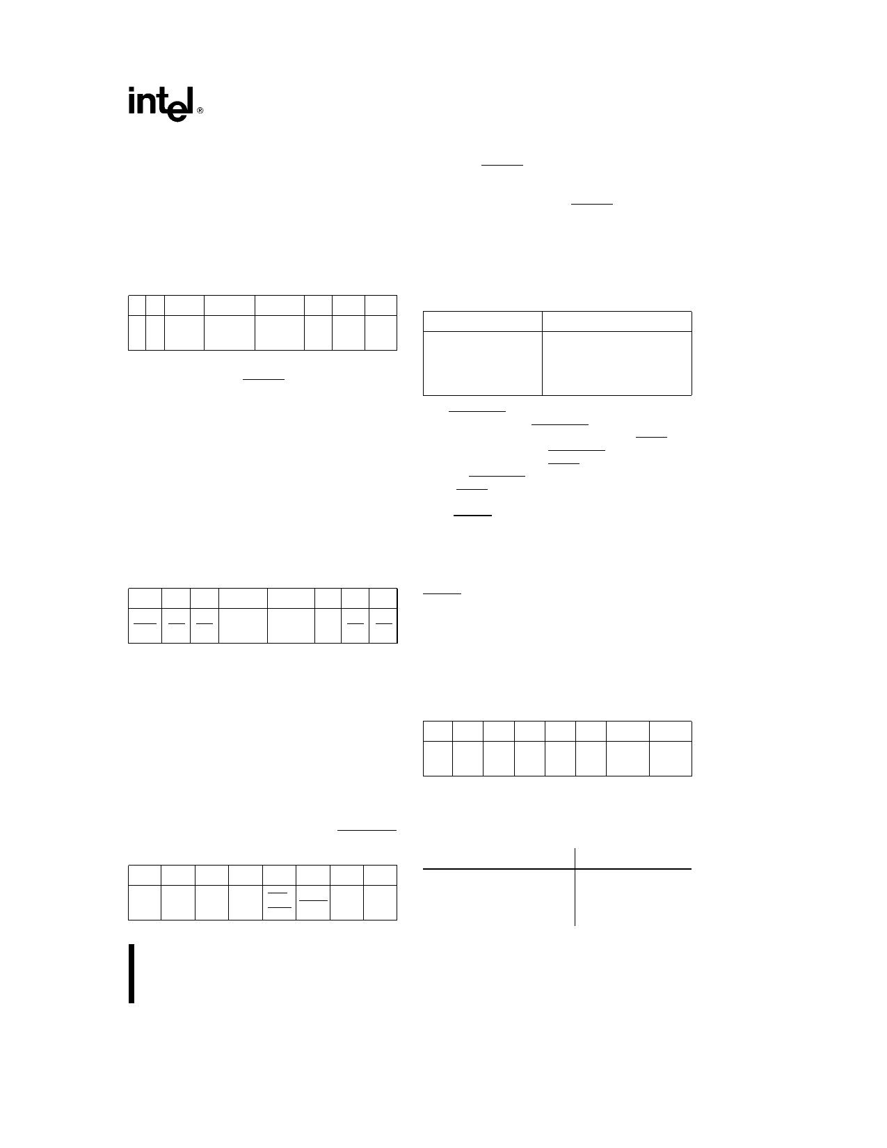
Table 2-1 lists a set of DOR values to activate the
drive select and motor enable for each drive
Table 2-1 Drive Activation Values
Drive
DOR Value
0
1CH
1
2DH
2
4EH
3
8FH
The DMAGATE bit is enabled only in PC-AT and
Model 30 Modes If DMAGATE is set low the INT
and DRQ outputs are tristated and the DACK and
TC inputs are disabled DMAGATE set high will en-
able INT DRQ TC and DACK to the system In PS
2 Mode DMAGATE has no effect upon INT DRQ
TC or DACK pins and they are always active
This RESET bit clears the basic core of the
82077AA and the FIFO circuits when the LOCK bit is
set to ‘‘0’’ (see section 5 3 2 for LOCK bit definition)
Once set it remains set until the user clears this bit
This bit is set by a chip reset and the 82077AA is
held in a reset state until the user clears this bit The
RESET bit has no effect upon this register
2 1 4 TAPE DRIVE REGISTER (TDR)
This register allows the user to assign tape support
to a particular drive during initialization Any future
references to that drive number automatically in-
vokes tape support This register is cleared by Hard-
ware reset Software resets have no effect
7
6
5
4
3
2
1
0
Tape
SEL1
Tape
SEL0
Bits 2 thru 7 are not writable and remain tristated if
read The Tape Select bits are Hardware RESET to
0’s making Drive 0 not available for tape support
Drive 0 is ‘‘reserved’’ for the floppy boot drive
Tape SEL1
0
0
1
1
Tape SEL0
0
1
0
1
DRIVE SELECTED
None
1
2
3
9
Share Link: 