RMWB24001 Ver la hoja de datos (PDF) - Raytheon Company
Número de pieza
componentes Descripción
Lista de partido
RMWB24001 Datasheet PDF : 6 Pages
| |||
RMWB24001
24 GHz Buffer Amplifier MMIC
Application
Information
PRODUCT INFORMATION
CAUTION: THIS IS AN ESD SENSITIVE DEVICE.
Chip carrier material should be selected to have GaAs compatible thermal coefficient of expansion and high thermal
conductivity such as copper molybdenum or copper tungsten. The chip carrier should be machined, finished flat,
plated with gold over nickel and should be capable of withstanding 325°C for 15 minutes.
Die attachment should utilize Gold/Tin (80/20) eutectic alloy solder and should avoid hydrogen environment for
PHEMT devices. Note that the backside of the chip is gold plated and is used as RF and DC ground.
These GaAs devices should be handled with care and stored in dry nitrogen environment to prevent contamination
of bonding surfaces. These are ESD sensitive devices and should be handled with appropriate precaution including
the use of wrist grounding straps. All die attach and wire/ribbon bond equipment must be well grounded to prevent
static discharges through the device.
Recommended wire bonding uses 3 mils wide and 0.5 mil thick gold ribbon with lengths as short as practical
allowing for appropriate stress relief. The RF input and output bonds should be typically 0.012” long corresponding
to a typically 2 mil between the chip and the substrate material.
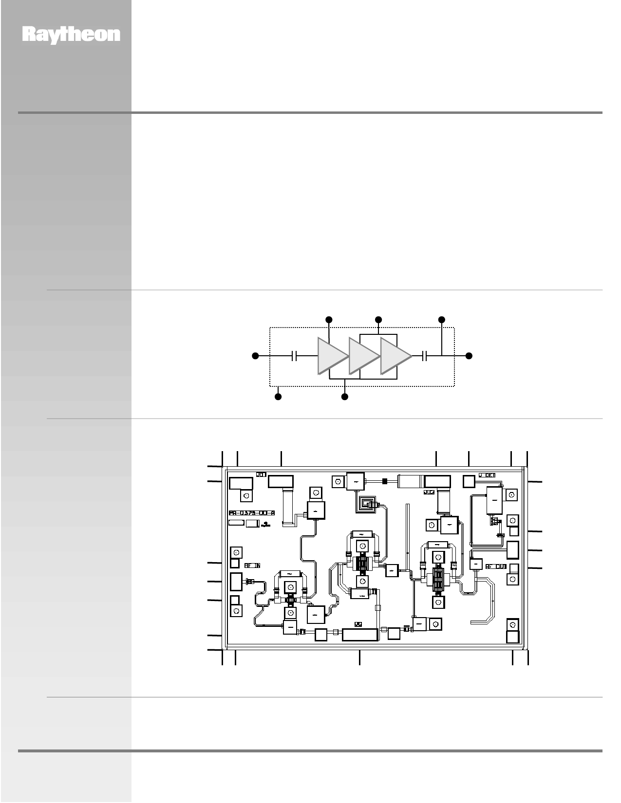
Figure 1
Functional Block
Diagram1
RF IN
Drain Supply Drain Supply Output Power
Vd1
Vd2 and Vd3 Detector Voltage Vdet
MMIC Chip
RF OUT
Ground (Back of Chip) Gate Supply Vg
Figure 2 Dimensions in millimeters
Chip Layout and Bond
Pad locations.
0.00 0.11
0.48
Chip size is 2.50 mm x
1.50
1.50 mm x 100 µm.
1.38
Back of chip is RF and
DC ground.
0.715
0.56
0.405
1.77 2.02
2.38 2.50
1.38
0.975
0.82
0.665
0.12
0.00
0.00 0.11
1.14
2.38 2.50
www.raytheon.com/micro
Note:
1. Detector delivers > 0 V DC into 3 kΩ load resistor for > +17 dBm output power. If output power level detection is not desired, do not
connect to detector bond pad.
Characteristic performance data and specifications are subject to change without notice.
Revised March 14, 2001
Page 2
Raytheon RF Components
362 Lowell Street
Andover, MA 01810
Share Link: 