CPV363M4K Ver la hoja de datos (PDF) - International Rectifier
Número de pieza
componentes Descripción
Lista de partido
CPV363M4K Datasheet PDF : 10 Pages
| |||
CPV363M4K
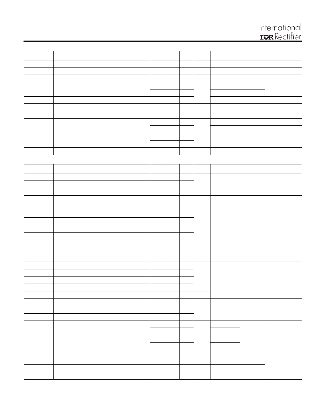
Electrical Characteristics @ TJ = 25°C (unless otherwise specified)
Parameter
Min. Typ. Max. Units
Conditions
V(BR)CES Collector-to-Emitter Breakdown Voltage 600 ––– ––– V VGE = 0V, IC = 250µA
∆V(BR)CES/∆TJ Temp. Coeff. of Breakdown Voltage
––– 0.45 ––– V/°C VGE = 0V, IC = 1.0mA
VCE(on)
Collector-to-Emitter Saturation Voltage ––– 1.72 2.10
IC = 6.0A
VGE = 15V
––– 2.00 ––– V IC = 11A
See Fig. 2, 5
––– 1.60 –––
IC = 6.0A, TJ = 150°C
VGE(th)
Gate Threshold Voltage
3.0 ––– 6.0
VCE = VGE, IC = 250µA
∆VGE(th)/∆TJ Temp. Coeff. of Threshold Voltage
––– -13 ––– mV/°C VCE = VGE, IC = 250µA
gfe
Forward Transconductance
3.0 6.0 ––– S VCE = 100V, IC = 12A
ICES
Zero Gate Voltage Collector Current ––– ––– 250 µA VGE = 0V, VCE = 600V
––– ––– 2500
VGE = 0V, VCE = 600V, TJ = 150°C
VFM
Diode Forward Voltage Drop
––– 1.4 1.7 V IC = 12A
See Fig. 13
––– 1.3 1.6
IC = 12A, TJ = 150°C
IGES
Gate-to-Emitter Leakage Current
––– ––– ±100 nA VGE = ±20V
Switching Characteristics @ TJ = 25°C (unless otherwise specified)
Parameter
Min. Typ. Max. Units
Conditions
Qg
Total Gate Charge (turn-on)
––– 61 91
IC = 6A
Qge
Gate - Emitter Charge (turn-on)
––– 7.4 11 nC VCC = 400V
Qgc
Gate - Collector Charge (turn-on)
––– 27 40
See Fig. 8
td(on)
Turn-On Delay Time
––– 55 –––
TJ = 25°C
tr
Rise Time
––– 24 ––– ns IC = 6.0A, VCC = 480V
td(off)
Turn-Off Delay Time
––– 107 160
VGE = 15V, RG = 23Ω
tf
Fall Time
Eon
Turn-On Switching Loss
––– 92 140
––– 0.28 –––
Energy losses include "tail" and
diode reverse recovery.
Eoff
Turn-Off Switching Loss
––– 0.10 ––– mJ See Fig. 9, 10, 18
Ets
Total Switching Loss
––– 0.39 0.50
tsc
Short Circuit Withstand Time
10 ––– ––– µs VCC = 360V, TJ = 125°C
td(on)
Turn-On Delay Time
––– 54 –––
VGE = 15V, RG = 23Ω, VCPK < 500V
TJ = 150°C, See Fig.10, 11, 18
tr
td(off)
Rise Time
Turn-Off Delay Time
––– 24 –––
––– 161 –––
ns IC = 6.0A, VCC = 480V
VGE = 15V, RG = 23Ω
tf
Fall Time
––– 244 –––
Energy losses include "tail" and
Ets
Total Switching Loss
Cies
Input Capacitance
––– 0.60 ––– mJ diode reverse recovery.
––– 740 –––
VGE = 0V
Coes
Output Capacitance
––– 100 ––– pF VCC = 30V
See Fig. 7
Cres
Reverse Transfer Capacitance
––– 9.3 –––
ƒ = 1.0MHz
trr
Diode Reverse Recovery Time
––– 42 60 ns TJ = 25°C See Fig.
––– 80 120
TJ = 125°C
14
IF = 12A
Irr
Diode Peak Reverse Recovery Current ––– 3.5 6.0 A TJ = 25°C See Fig.
––– 5.6 10
TJ = 125°C
15
VR = 200V
Qrr
Diode Reverse Recovery Charge
––– 80 180 nC TJ = 25°C See Fig.
––– 220 600
TJ = 125°C
16 di/dt=200A/µs
d i(rec)M / dt Diode Peak Rate of Fall of Recovery
During tb
––– 180 ––– A/µs TJ = 25°C See Fig.
––– 120 –––
TJ = 125°C
17
Notes:
Repetitive rating; VGE=20V, pulse width limited
by max. junction temperature. ( See fig. 20)
VCC=80%(VCES), VGE=20V, L=10µH,
RG= 23Ω, ( See fig. 19 )
Pulse width 5.0µs,
single shot.
Pulse width ≤ 80µs; duty factor ≤ 0.1%.
Share Link: 