CY7C008V(2010) Ver la hoja de datos (PDF) - Cypress Semiconductor
Número de pieza
componentes Descripción
Lista de partido
CY7C008V Datasheet PDF : 23 Pages
| |||
CY7C008V/009V
CY7C018V/019V
Switching Characteristics
Over the Operating Range[11] (continued)
Parameter
Description
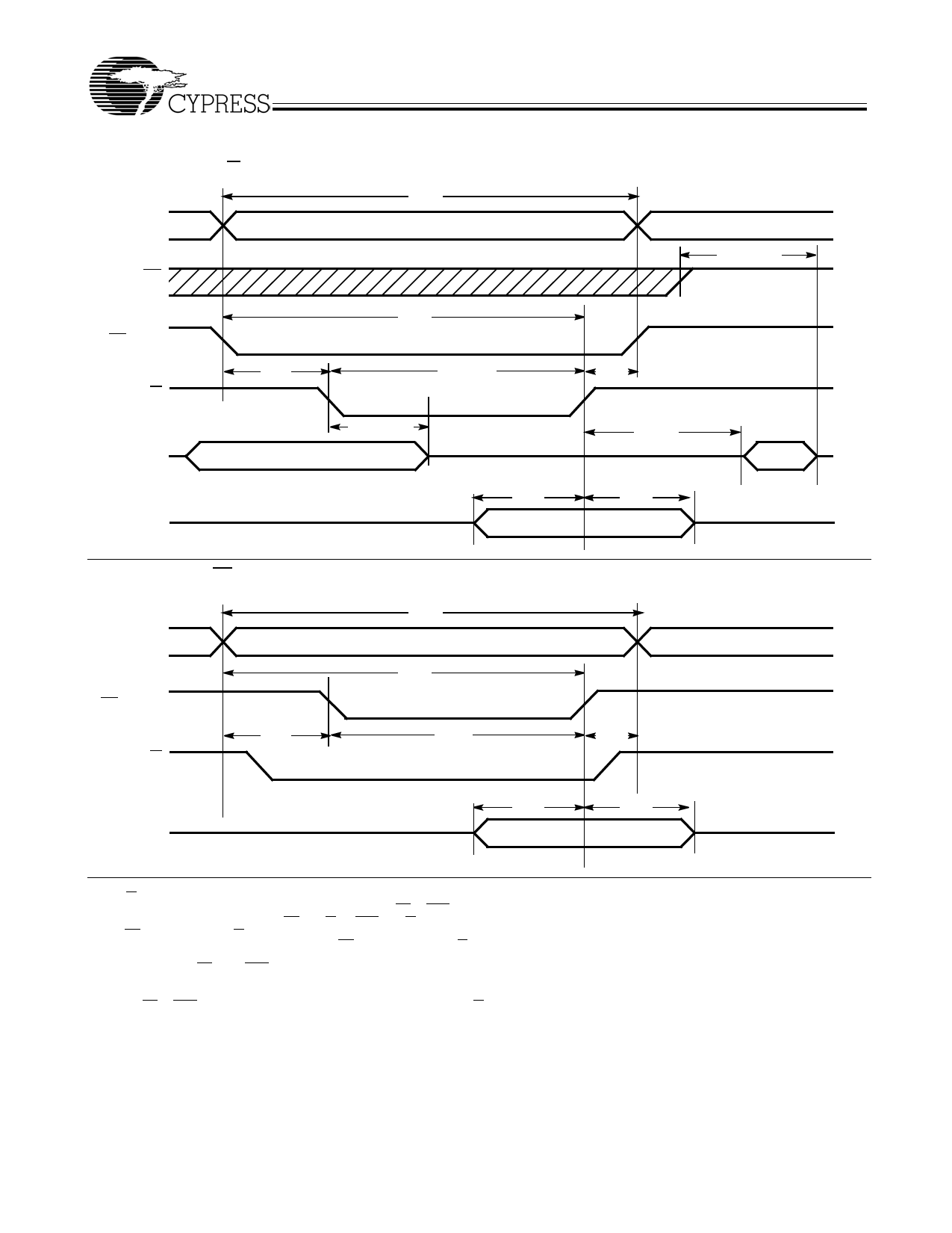
WRITE CYCLE
tWC
tSCE[16]
Write cycle time
CE LOW to write end
tAW
Address valid to write end
tHA
tSA[16]
Address hold from write end
Address set-up to write start
tPWE
Write pulse width
tSD
Data set-up to write end
tHD
Data hold from write end
tHZWE[17, 18]
R/W LOW to high Z
tLZWE[17, 18]
R/W HIGH to low Z
tWDD[19]
Write pulse to data delay
tDDD[19]
Write data valid to read data valid
BUSY TIMING[20]
tBLA
BUSY LOW from address match
tBHA
BUSY HIGH from address mismatch
tBLC
BUSY LOW from CE LOW
tBHC
BUSY HIGH from CE HIGH
tPS
Port set-up for priority
tWB
R/W HIGH after BUSY (Slave)
tWH
R/W HIGH after BUSY HIGH (Slave)
tBDD[21]
BUSY HIGH to data valid
INTERRUPT TIMING[20]
tINS
INT set time
tINR
INT reset time
SEMAPHORE TIMING
tSOP
tSWRD
tSPS
tSAA
SEM flag update pulse (OE or SEM)
SEM flag write to read time
SEM flag contention window
SEM address access time
CY7C018V/019V
–15
–20
–25
Unit
Min Max Min Max Min Max
15
–
20
–
25
–
ns
12
–
16
–
20
–
ns
12
–
16
–
20
–
ns
0
–
0
–
0
–
ns
0
–
0
–
0
–
ns
12
–
17
–
22
–
ns
10
–
12
–
15
–
ns
0
–
0
–
0
–
ns
–
10
–
12
–
15
ns
3
–
3
–
3
–
ns
–
30
–
40
–
50
ns
–
25
–
30
–
35
ns
–
15
–
20
–
20
ns
–
15
–
20
–
20
ns
–
15
–
20
–
20
ns
–
15
–
16
–
17
ns
5
–
5
–
5
–
ns
0
–
0
–
0
–
ns
13
–
15
–
17
–
ns
–
15
–
20
–
25
ns
–
15
–
20
–
20
ns
–
15
–
20
–
20
ns
10
–
10
–
12
–
ns
5
–
5
–
5
–
ns
5
–
5
–
5
–
ns
–
15
–
20
–
25
ns
Notes
16. To access RAM, CE = L, UB = L, SEM = H. To access semaphore, CE = H and SEM = L. Either condition must be valid for the entire tSCE time.
17. Test conditions used are Load 2.
18. This parameter is guaranteed by design, but it is not production tested.For information on port-to-port delay through RAM cells from writing port to reading port,
refer to Read Timing with Busy waveform.
19. For information on port-to-port delay through RAM cells from writing port to reading port, refer to Read Timing with Busy waveform.
20. Test conditions used are Load 1.
21. tBDD is a calculated parameter and is the greater of tWDD–tPWE (actual) or tDDD–tSD (actual).
Document Number: 38-06044 Rev. *E
Page 9 of 23
[+] Feedback
Share Link: 