AN-6920MR Ver la hoja de datos (PDF) - Fairchild Semiconductor
Número de pieza
componentes Descripción
Lista de partido
AN-6920MR
Fairchild Semiconductor

AN-6920MR Datasheet PDF : 17 Pages
| |||
AN-6920
Lm
=
η
⋅ (VO.PFC.L ⋅ Dmax )2
2⋅
f min
s.QR
⋅
PO
=
0.95 ⋅ (300 ⋅ 0.413)2
2 ⋅ 70 ×103 ⋅ 90
= 1160µH
I PK
DS
=
VO.PFC.L ⋅ Dmax
L f min
m S .QR
=
300 ⋅ 0.413
1160 ×10−6 ⋅ 70 ×
103
= 1.53A
tOFF . L
=
(1− Dmax )
f min
S .QR
=
1− 0.413
70 ×103
=
8.39µs
tOFF .H
=
tOFF .L
⋅
VO . PFC . L
VO.PFC.H
⋅ VO.PFC.H
VO.PFC.L
+ VRO
+ VRO
= 8.39 ×10−6 ⋅ 300 ⋅ 400 + 240 = 7.46µs > 5µs
400 300 + 240
Assuming QP2912 (Ae=144mm2) core is used and the flux
swing is 0.28T
N min
P
=
Lm I DS PK
Ae∆B
1160 ×10−6 ⋅1.53
= 144 ×10−6 ⋅ 0.28 = 44
NP
=
n⋅
NS
⇒ 12 ⋅ 3
=
36
<
N min
P
⇒ 12 ⋅ 4 = 48 > NPmin
NP is determined as 48, NS is 4.
12
(VO
+ VFA
+ VF )
⋅
N
S
<
N AUX
<
20
(VO
+ VFA
+VF )
⋅
N
S
12 +1
20 +1
⇒ 20 ⋅ 4 < N AUX < 20 ⋅ 4
⇒ 2.6 < N AUX < 4.2
Thus, NAUX is determined as 3.
The number of turns of the high-side driver auxiliary is
given as:
NAUX.H ≦ NAUX
NAUX.H is determined as 2.
Assuming the pulse-by-pulse current limit for low PFC
output voltage is 140% of peak drain current at heavy load:
Bmax
=
Lm I LIM
Ae N P
1160×10−6 ⋅ 2.14
= 144 ×10−6 ⋅ 48 = 0.36T
APPLICATION NOTE
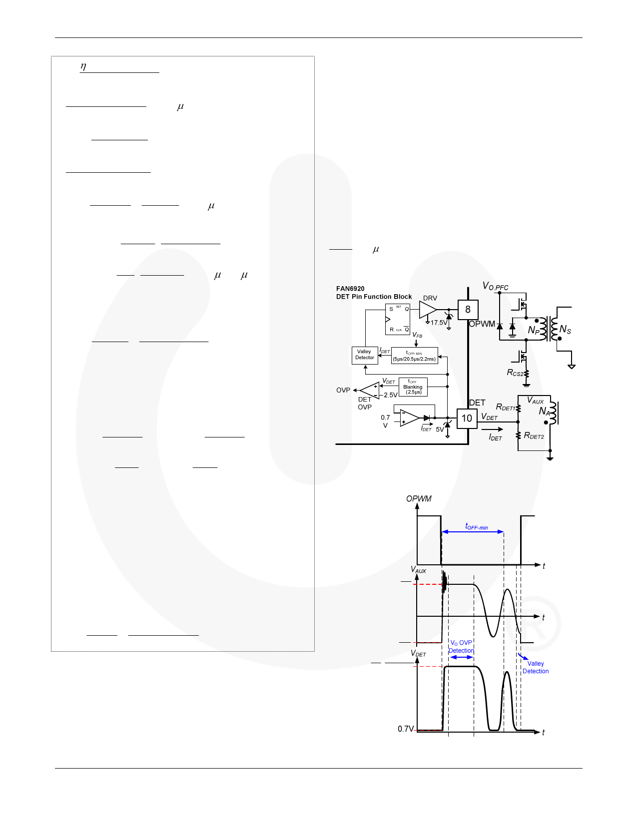
[STEP-B3] Design the Valley Detection Circuit
The valley of MOSFET voltage is detected by monitoring
the current flowing out of the DET pin. The typical
application circuit is shown as Figure 15 and typical
waveforms are shown in Figure 16. The DET pin has upper
and lower voltage clamping at 5V and 0.7V, respectively. The
valley detection circuit is blanked for 5µs after the
MOSFET is turned off. When VAUX drops below zero, VDET
is clamped at 0.7V and current flows out of the DET pin.
MOSFET is turned on with 200ns delay once the current
flowing out of DET pin exceeds 30µA. To guarantee that
valley detection circuit is triggered when the DET pin is
clamped at 0.7V, the current flowing through RDET2 should
be larger than 30µA as:
0.7 > 30µ A
RDET 2
(30)
Figure 15. Typical Application Circuit of DET Pin
VO
⋅
NA
NS
− VO .PFC
⋅
NA
NP
VO
⋅
NA
NS
⋅
RA
RDET +
RA
© 2010 Fairchild Semiconductor Corporation
Rev. 1.0.0 • March 10, 2011
Figure 16. Waveforms of Valley Detection and
VO OVP Detection
www.fairchildsemi.com
10
Share Link: