AN-6920MR Ver la hoja de datos (PDF) - Fairchild Semiconductor
Número de pieza
componentes Descripción
Lista de partido
AN-6920MR
Fairchild Semiconductor

AN-6920MR Datasheet PDF : 17 Pages
| |||
AN-6920
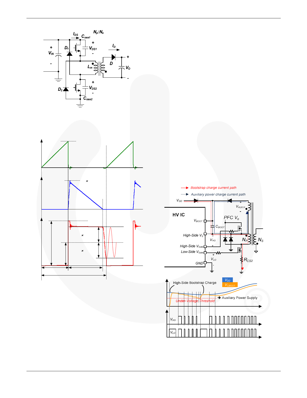
Figure 6. Schematic of Dual-Switch Flyback Converter
Ids (MOSFET Drain-to-Source Current)
Ipk
ID (Diode Current)
Ipk Np/Ns
APPLICATION NOTE
and low cost. The bootstrap circuit is useful in a high-
voltage gate driver and operates as follows. When the high-
side VS goes below the IC supply voltage VDD or is pulled
down to ground (the low-side switch is turned on and the
high-side switch is turned off), the bootstrap capacitor,
CBOOT, charges through the transformer primary-side, from
the VDD power supply, as shown in Figure 8. This is
provided by VBS when high-side VS is pulled to a higher
voltage by the high-side switch. The VBS supply floats and
the bootstrap diode reverses bias and blocks the rail voltage
(the low-side switch is turned off and high-side switch is
turned on) from the IC supply voltage, VDD. However, the
dual-switch flyback high-side and low-side MOSFET turn
on and off at the same time. Therefore, once the high-side
MOSFET turns on, high-side VS equals PFC VO, the VDD
can’t charge the CBOOT, even though the high-side VS is
pulled down to ground at leakage energy recycle period, but
the period is too short to charge CBOOT.
Figure 8 shows the high-side gate-driver circuit with the
auxiliary power supply. If VCBOOT is less than the HV IC
under-voltage threshold, the high-side gate output (VHO)
maintains turned-off state, then the low-side MOSFET turns
on and charges the CBOOT for one cycle, high-side driver
restarts at the next PWM cycle. Finally, the voltage of
auxiliary power supply follows the output voltage rise and
continues to supply energy to the high-side circuit.
Vds
VIN
VIN /2
Vo/2 Np/Ns
Vo/2 Np/Ns
tON
tD
tS
Figure 7. Typical Waveforms of Dual-Switch QR
Flyback Converter
4. High-Side Gate-Drive Circuit
Figure 8 and Figure 9 show the high/low-side gate driver
circuit. The high-side gate drive IC achieves high-
performance, is simple and inexpensive, but has a limitation
for dual-switch flyback application.
One of the most widely used methods to supply power to
the high-side gate driver circuitry of the high-voltage gate-
drive IC is the bootstrap power supply. This bootstrap
power supply technique has the advantage of being simple
Figure 8. High-Side Driver Circuit and Start Waveform
© 2010 Fairchild Semiconductor Corporation
Rev. 1.0.0 • March 10, 2011
4
www.fairchildsemi.com
Share Link: