AN-6920MR Ver la hoja de datos (PDF) - Fairchild Semiconductor
Número de pieza
componentes Descripción
Lista de partido
AN-6920MR
Fairchild Semiconductor

AN-6920MR Datasheet PDF : 17 Pages
| |||
AN-6920
APPLICATION NOTE
(Design Example) Since the output voltage is 400V, the
minimum frequency occurs at high-line (264VAC) and full-
load condition. Assuming the overall efficiency is 90% and
selecting the minimum frequency as 50kHz, the inductor
value is obtained as:
L=
η ⋅V 2
LINE,MAX
⋅ VO.PFC.H − 2 ⋅VLINE,MAX
2 ⋅ POUT ⋅ fSW ,MIN
VO.PFC
=
0.9 ⋅ 2642
2 ⋅ 90 ⋅ 50 ×103
⋅
400
−2
400
⋅
264
=
464µH
The inductance of boot inductor is determined as
450µH.
The maximum peak inductor current at nominal output
power is calculated as:
I L,PK
2
=
2 ⋅ POUT
η ⋅VLINE,MIN
= 2 2 ⋅90 = 3.14A
0.9 ⋅ 90
t MAX
ON
=
2 ⋅ POUT ⋅ L
η ⋅V 2
LINE.MIN
=
2 ⋅ 90 ⋅ 450 ×10−6
0.9 ⋅ 902
= 11.1µs < 20µs
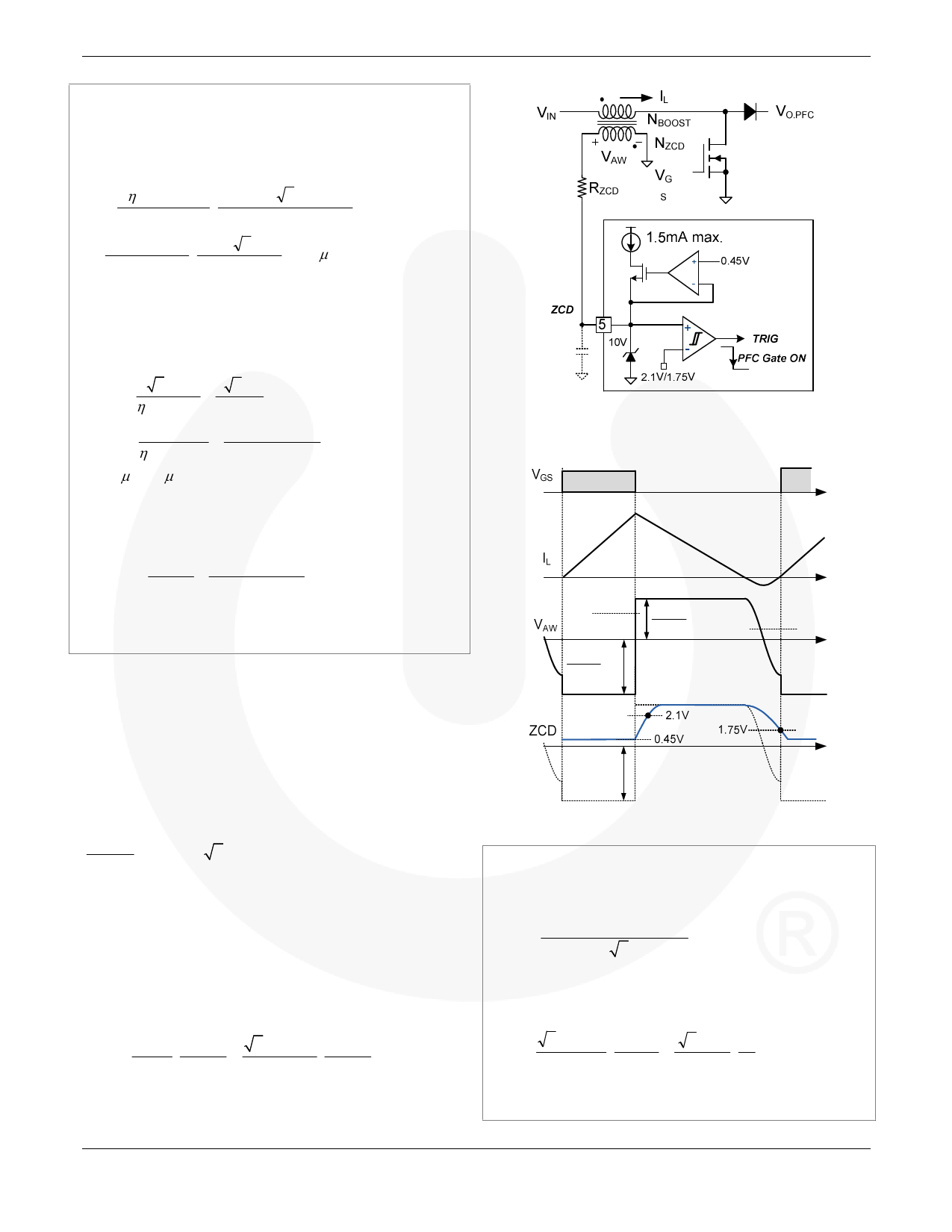
Figure 10.Internal Block for ZCD
Assuming QP2512 core (3C96, Ae=110mm2) is used and
setting ∆B as 0.30T, the primary winding should be:
N BOOST
≥
I L,PK ⋅ L
Ae ⋅ ∆B
=
3.14× 450×10−6
110×10−6 × 0.30
=
42.82turns
Thus, the number of turns (NBOOST) of boost inductor is
determined as 44.
[STEP-A2] Auxiliary Winding Design
Figure 11 shows the internal block for zero-current
detection (ZCD) for the PFC. FAN6920 indirectly detects
the inductor zero current instant using an auxiliary winding
of the boost inductor.
The auxiliary winding should be designed such that the
voltage of the ZCD pin rises above 2.1V when the boost
switch is turned off to trigger internal comparator as:
N ZCD
N BOOST
(VO. PFC . H
−
2VLINE.MAX ) > 2.1V
(10)
where VO.PFC.H is the PFC output voltage for high line
condition.
The ZCD pin has upper and lower voltage clamping at 10V
and 0.45V, respectively. When ZCD pin voltage is clamped
at 0.45V, the maximum sourcing current is 1.5mA and,
therefore, the resistor RZCD should be designed to limit the
current of the ZCD pin below 1.5mA in the worst case as:
RZCD
>
VIN ⋅
1.5mA
N AUX
N BOOST
=
2VLINE.MAX ⋅ N AUX
1.5mA NBOOST
(11)
N ZCD
N BOOST
VIN
NZCD
N BOOST
(VO.PFC
−VIN )
Figure 11. ZCD Waveforms
(Design Example) The number of turns for the auxiliary
ZCD winding is obtained as:
N ZCD
>
2.1N BOOST
(VO.PFC.H − 2VLINE.MAX
)
= 3.5turns
With a margin, NAUX is determined as 8 turns.
Then RZCD is selected from:
RZCD >
2VLINE MAX
1.5mA
⋅ N ZCD
N BOOST
2 ⋅ 264
= 1.5×10−3
⋅ 8 = 45.248kΩ
44
as 47.5kΩ.
© 2010 Fairchild Semiconductor Corporation
Rev. 1.0.0 • March 10, 2011
6
www.fairchildsemi.com
Share Link: