IDT72205LB Ver la hoja de datos (PDF) - Integrated Device Technology
Número de pieza
componentes Descripción
Lista de partido
IDT72205LB
Integrated Device Technology

IDT72205LB Datasheet PDF : 21 Pages
| |||
IDT72205LB/72215LB/72225LB/72235LB/72245LB CMOS SyncFIFO™
256 x 18-BIT, 512 x 18, 1024 x 18, 2048 x 18 and 4096 x 18
AC TEST CONDITIONS
Input Pulse Levels
Input Rise/Fall Times
Input Timing Reference Levels
Output Reference Levels
Output Load
GND to 3.0V
3ns
1.5V
1.5V
See Figure 1
2766 tbl 07
MILITARY AND COMMERCIAL TEMPERATURE RANGES
5V
D.U.T.
680Ω
1.1K
30pF*
SIGNAL DESCRIPTIONS:
INPUTS:
DATA IN (D0 - D17)
Data inputs for 18-bit wide data.
CONTROLS:
RESET (RS)
Reset is accomplished whenever the Reset (RS) input is
taken to a LOW state. During reset, both internal read and
write pointers are set to the first location. A reset is required
after power-up before a write operation can take place. The
Full Flag (FF), Half-Full Flag (HF), and Programmable Almost-
Full Flag (PAF) will be reset to HIGH after tRSF. The Empty
Flag (EF) and Programmable Almost-Empty Flag (PAE) will be
reset to LOW after tRSF. During reset, the output register is
initialized to all zeros and the offset registers are initialized to
their default values.
WRITE CLOCK (WCLK)
A write cycle is initiated on the LOW-to-HIGH transition of
the write clock (WCLK). Data set-up and hold times must be
met with respect to the LOW-to-HIGH transition of the write
clock (WCLK).
The write and read clocks can be asynchronous or
coincident.
WRITE ENABLE (WEN)
When Write Enable (WEN) is LOW, data can be loaded into
the input register and RAM array on the LOW-to-HIGH transi-
tion of every write clock (WCLK). Data is stored in the RAM
array sequentially and independently of any on-going read
operation.
When WEN is HIGH, the input register holds the previous
data and no new data is loaded into the FIFO.
To prevent data overflow, the Full Flag (FF) will go LOW,
inhibiting further write operations. Upon the completion of a
valid read cycle, the FF will go HIGH after tWFF allowing a write
to begin. WEN is ignored when the FIFO is full.
READ CLOCK (RCLK)
Data can be read on the outputs on the LOW-to-HIGH
transition of the read clock (RCLK), when Output Enable (OE)
is set LOW.
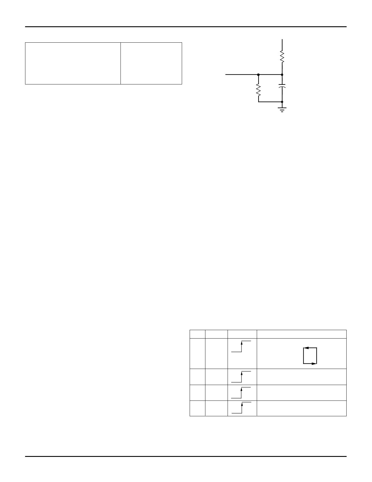
2766 drw 05
Figure 1. Output Load
* Includes jig and scope capacitances.
The write and read clocks can be asynchronous or
coincident.
READ ENABLE (REN)
When Read Enable (REN) is LOW, data is loaded from the
RAM array to the output register on the LOW-to-HIGH transi-
tion of the read clock (RCLK).
When REN is HIGH, the output register holds the previous
data and no new data is loaded into the register.
When all the data has been read from the FIFO, the Empty
Flag (EF) will go LOW, inhibiting further read operations. Once
a write is performed, the EF will go HIGH after tREF and a read
can begin. REN is ignored when the FIFO is empty.
OUTPUT ENABLE (OE)
When Output Enable (OE) is enabled (LOW), the parallel
output buffers receive data from the output register. When OE
is disabled (HIGH), the Q output data bus is in a high-
impedance state.
LOAD (LD)
The IDT72205LB/72215LB/72225LB/72235LB/72245LB
devices contain two 12-bit offset registers with data on the
inputs, or read on the outputs. When the Load (LD) pin is set
LOW and WEN is set LOW, data on the inputs D0-D11 is
written into the Empty offset register on the first LOW-to-HIGH
transition of the write clock (WCLK). When the LD pin and
LD WEN
0
0
WCLK(1)
Selection
Writing to offset registers:
Empty Offset
Full Offset
0
1
No Operation
1
0
Write Into FIFO
1
1
No Operation
NOTE:
2766 tbl 08
1. The same selection sequence applies to reading from the registers. REN
is enabled and read is performed on the LOW-to-HIGH transition of RCLK.
Figure 2. Write Offset Register
5.16
7
Share Link: