IDT72265LA Ver la hoja de datos (PDF) - Integrated Device Technology
Número de pieza
componentes Descripción
Lista de partido
IDT72265LA Datasheet PDF : 27 Pages
| |||
IDT72255LA/72265LA SUPERSYNC FIFO™
8,192 x 18, 16,384 x 18
COMMERCIAL AND INDUSTRIAL TEMPERATURE RANGE
72255LA – 8,192 x 18–BIT
17
12
72265LA – 16,384 x 18–BIT
0
17
13
0
EMPTY OFFSET REGISTER
DEFAULT VALUE
07FH if is LOW at Master Reset,
3FFH if is HIGH at Master Reset
EMPTY OFFSET REGISTER
DEFAULT VALUE
07FH if is LOW at Master Reset,
3FFH if is HIGH at Master Reset
17
12
0
17
13
0
FULL OFFSET REGISTER
DEFAULT VALUE
07FH if is LOW at Master Reset,
3FFH if is HIGH at Master Reset
FULL OFFSET REGISTER
DEFAULT VALUE
07FH if is LOW at Master Reset,
3FFH if is HIGH at Master Reset
4670 drw 06
Figure 3. Offset Register Location and Default Values
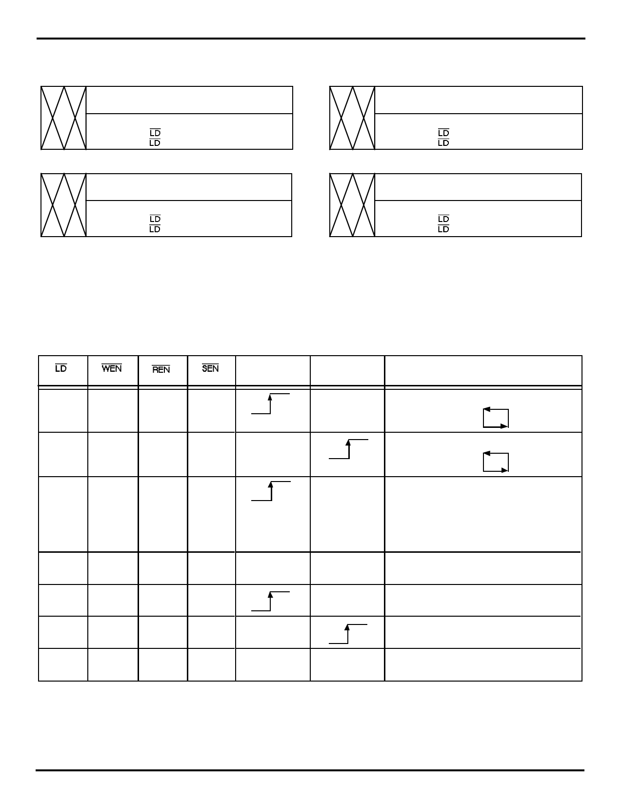
WCLK
RCLK
Selection
0
0
1
1
0
1
0
1
X
0
1
1
0
X
1
1
1
X
X
Parallel write to registers:
Empty Offset
Full Offset
Parallel read from registers:
Empty Offset
Full Offset
X
Serial shift into registers:
26 bits for the 72255LA
28 bits for the 72265LA
1 bit for each rising WCLK edge
Starting with Empty Offset (LSB)
Ending with Full Offset (MSB)
X
No Operation
1
0
X
X
X
Write Memory
1
X
0
X
X
1
1
1
X
X
Read Memory
X
No Operation
NOTES:
1. The programming method can only be selected at Master Reset.
2. Parallel reading of the offset registers is always permitted regardless of which programming method has been selected.
3. The programming sequence applies to both IDT Standard and FWFT modes.
Figure 4. Programmable Flag Offset Programming Sequence
4670 drw 07
9
Share Link: 