LH540215 Ver la hoja de datos (PDF) - Sharp Electronics
Número de pieza
componentes Descripción
Lista de partido
LH540215 Datasheet PDF : 48 Pages
| |||
512 x 18/1024 x 18 Synchronous FIFO
LH540215/25
PIN DESCRIPTIONS (cont’d)
PIN
NAME
PIN
TYPE 1
DESCRIPTION
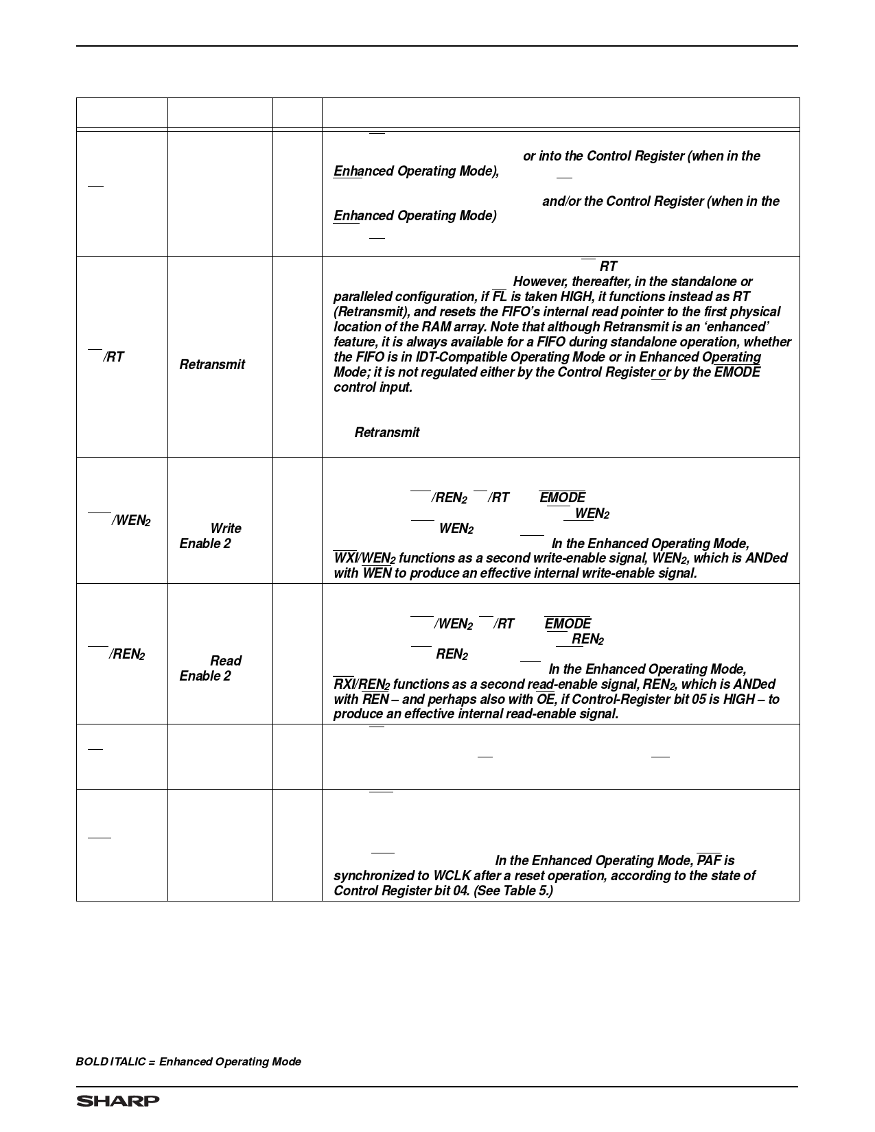
LD
Load
When LD is LOW, the data word on D0 – D17 (the data inputs) is written into a
programmable-flag-offset register, or into the Control Register (when in the
Enhanced Operating Mode), on the LOW-to-HIGH transition of WCLK, whenever
I
WEN is LOW. (See Table 3.) Also, when LD is LOW, a word is read to Q0 – Q17 (the
data outputs) from the offset registers and/or the Control Register (when in the
Enhanced Operating Mode) on the LOW-to-HIGH transition of RCLK, whenever
REN is LOW. (See again Table 3, and particularly the Notes following this table.)
When LD is HIGH, normal FIFO write and read operations are enabled.
FL/RT
First Load/
Retransmit
In the standalone or paralleled configuration, FL/RT should be LOW during a reset
operation. (See Tables 1 and 2.) However, thereafter, in the standalone or
paralleled configuration, if FL is taken HIGH, it functions instead as RT
(Retransmit), and resets the FIFO’s internal read pointer to the first physical
location of the RAM array. Note that although Retransmit is an ‘enhanced’
feature, it is always available for a FIFO during standalone operation, whether
I
the FIFO is in IDT-Compatible Operating Mode or in Enhanced Operating
Mode; it is not regulated either by the Control Register or by the EMODE
control input. In IDT-compatible cascaded configuration, FL has an entirely
different function; it is grounded for the first FIFO device (the ‘master’ device or ‘first-
load’ device), and is set to HIGH for all other FIFO devices in the daisy chain. Thus,
the Retransmit feature is not available for FIFOs operating in an IDT-compatible
cascaded configuration.
WXI/WEN2
Write
Expansion
Input/Write
Enable 2
This signal is dual-purpose; its functionality is determined during a reset operation,
according to its own state, and also according to the states of the three other
control inputs RXI/REN2, FL/RT, and EMODE. (See Tables 1 and 2.) In the
I
standalone or paralleled configuration, WXI/WEN2 is grounded. In the cascaded
configuration, WXI/WEN2 is connected to WXO (Write Expansion Output) of the
previous device, and functions as WXI. In the Enhanced Operating Mode,
WXI/WEN2 functions as a second write-enable signal, WEN2, which is ANDed
with WEN to produce an effective internal write-enable signal. 2
RXI/REN2
Read
Expansion
Input/Read
Enable 2
This signal is dual-purpose; its functionality is determined during a reset operation,
according to its own state, and also according to the states of the three other
control inputs WXI/WEN2, FL/RT, and EMODE. (See Tables 1 and 2.) In the
standalone or paralleled configuration, RXI/REN2 is grounded. In the cascaded
I
configuration, RXI/REN2 is connected to RXO (Read Expansion Output) of the
previous device, and functions as RXI. In the Enhanced Operating Mode,
RXI/REN2 functions as a second read-enable signal, REN2, which is ANDed
with REN – and perhaps also with OE, if Control-Register bit 05 is HIGH – to
produce an effective internal read-enable signal. 2
When FF is LOW, the FIFO is full; further advancement of its internal write-address
FF
Full Flag
O
pointer, and further data writes through its Data Inputs into its internal memory
array, are inhibited. When FF is HIGH, the FIFO is not full. FF is synchronized to
WCLK.
When PAF is LOW, the FIFO is ‘almost full,’ based on the almost-full-offset value
programmed into the FIFO’s Almost-Full Offset Register. The default value of this
PAF
Programmable
Almost-Full Flag
O
offset at reset is one-eighth of the total number of words in the FIFO-memory array,
minus one, measured from ‘full.’ (See Table 4.) In the IDT-Compatible Operating
Mode, PAF is asynchronous. In the Enhanced Operating Mode, PAF is
synchronized to WCLK after a reset operation, according to the state of
Control Register bit 04. (See Table 5.)
NOTES:
1. I = Input, O = Output, Z = High-Impedance, V = Power Voltage Level
2. The ostensible differences in signal assertiveness are reconciled before ANDing.
BOLD ITALIC = Enhanced Operating Mode
7
Share Link: 