LT3082 Ver la hoja de datos (PDF) - Linear Technology
Número de pieza
componentes Descripción
Lista de partido
LT3082 Datasheet PDF : 20 Pages
| |||
LT3082
PIN FUNCTIONS (DD/ST/TS8)
IN (Pins 7, 8/Pin 3/Pins 7, 8): Input. This pin supplies
power to regulate internal circuitry and supply output load
current. For the device to operate properly and regulate,
the voltage on this pin must be 1.2V to 1.4V above the
OUT pin (depending on output load current—see the
dropout voltage specifications in the Electrical Charac-
teristics table).
NC (Pins 3, 5, 6/NA/Pins 1, 6): No Connection. These
pins have no connection to internal circuitry and may be
tied to IN, OUT, GND or floated.
OUT (Pins 1, 2/Pin 2/Pins 2, 3, 4): Output. This is the
power output of the device. The LT3082 requires a 0.5mA
minimum load current or the output will not regulate.
SET (Pin 4/Pin 1/Pin 5): Set. This pin is the error ampli-
fier’s noninverting input and also sets the operating bias
point of the circuit. A fixed 10μA current source flows
out of this pin. A single external resistor programs VOUT.
Output voltage range is 0V to 38.5V.
Exposed Pad/Tab (Pin 9/Tab/NA): Output. The Exposed
Pad of the DFN package and the Tab of the SOT-223
package are tied internally to OUT. Tie them directly to OUT
pins (Pins 1, 2/Pin 2) at the PCB. The amount of copper area
and planes connected to the Exposed Pad/Tab determine
the effective thermal resistance of the packages (see the
Applications Information section).
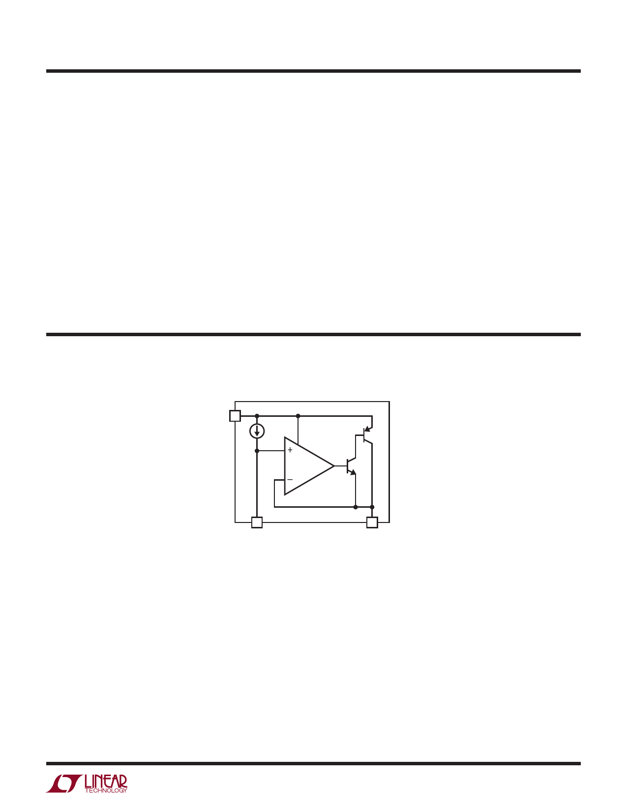
BLOCK DIAGRAM
IN
10μA
+
–
SET
OUT
3082 BD
3082f
7
Share Link: 