LT3082 Ver la hoja de datos (PDF) - Linear Technology
Número de pieza
componentes Descripción
Lista de partido
LT3082 Datasheet PDF : 20 Pages
| |||
LT3082
APPLICATIONS INFORMATION
Table 1. 1% Resistors for Common Output Voltages
VOUT (V)
1
RSET (k)
100
1.2
121
1.5
150
1.8
182
2.5
249
3.3
332
5
499
With a 10μA current source generating the reference
voltage, leakage paths to or from the SET pin can create
errors in the reference and output voltages. High qual-
ity insulation should be used (e.g., Teflon, Kel-F). The
cleaning of all insulating surfaces to remove fluxes and
other residues may be required. Surface coating may be
necessary to provide a moisture barrier in high humidity
environments.
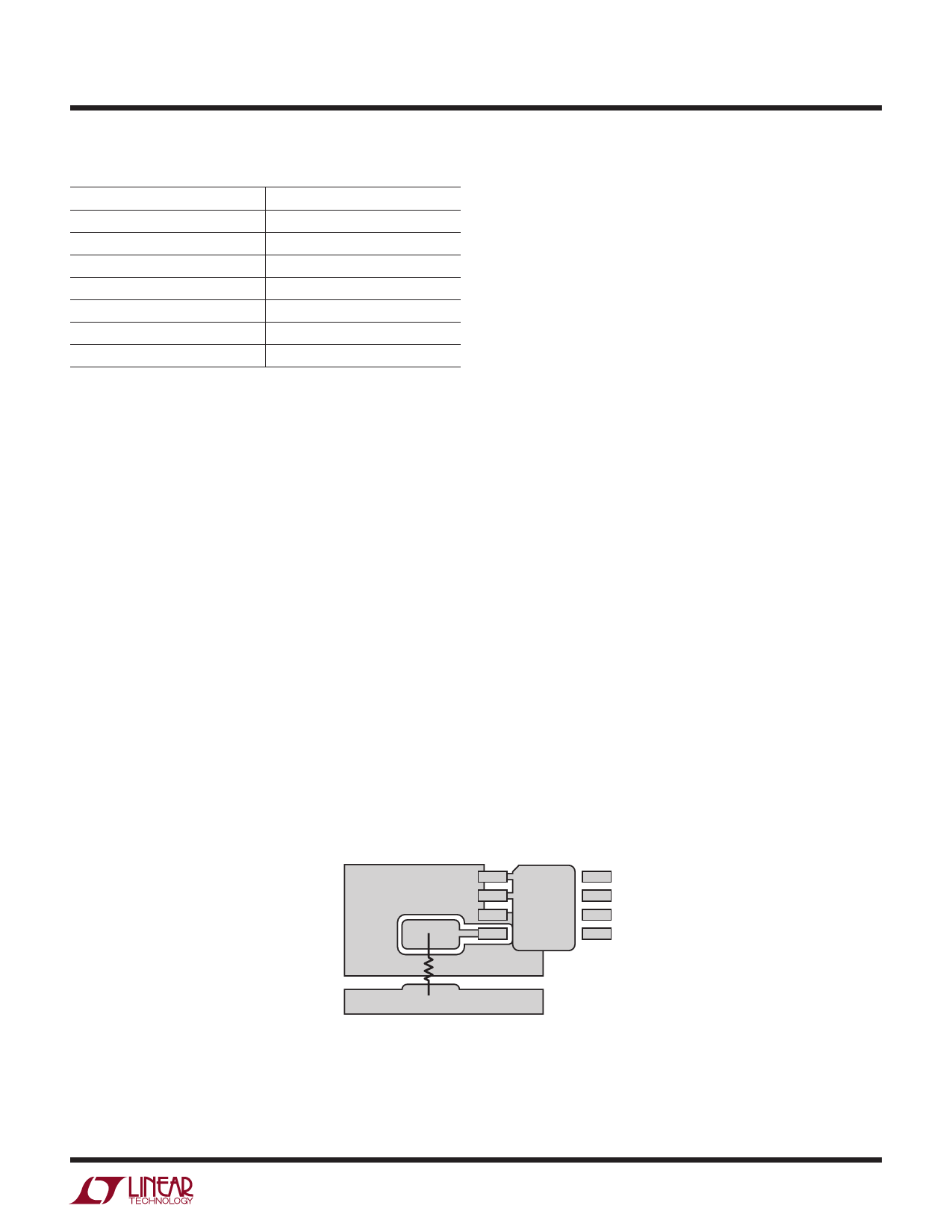
Minimize board leakage by encircling the SET pin and
circuitry with a guard ring that is operated at a potential
close to itself. Tie the guard ring to the OUT pin. Guarding
both sides of the circuit board is required. Bulk leakage
reduction depends on the guard ring width. 10nA of leak-
age into or out of the SET pin and its associated circuitry
creates a 0.1% reference voltage error. Leakages of this
magnitude, coupled with other sources of leakage, can
cause significant offset voltage and reference drift, es-
pecially over the possible operating temperature range.
Figure 2 depicts an example guard ring layout.
If guard ring techniques are used, this bootstraps any
stray capacitance at the SET pin. Since the SET pin is
a high impedance node, unwanted signals may couple
into the SET pin and cause erratic behavior. This will
be most noticeable when operating with minimum
output capacitors at full load current. The easiest way
to remedy this is to bypass the SET pin with a small
amount of capacitance from SET to ground; 10pF to
20pF is sufficient.
Stability and Output Capacitance
The LT3082 requires an output capacitor for stability. It
is designed to be stable with most low ESR capacitors
(typically ceramic, tantalum or low ESR electrolytic). A
minimum output capacitor of 2.2μF with an ESR of 0.5Ω
or less is recommended to prevent oscillations. Larger
values of output capacitance decrease peak deviations
and provide improved transient response for larger load
current changes. Bypass capacitors, used to decouple
individual components powered by the LT3082, increase
the effective output capacitor value. For improvement in
transient response performance, place a capacitor across
the voltage setting resistor. Capacitors up to 1μF can be
used. This bypass capacitor reduces system noise as well,
but start-up time is proportional to the time constant of
the voltage setting resistor (RSET in Figure 1) and SET pin
bypass capacitor.
Give extra consideration to the use of ceramic capacitors.
Ceramic capacitors are manufactured with a variety of di-
OUT
SET
GND
3082 F02
Figure 2. Example Guard Ring Layout for DFN Package
3082f
9
Share Link: 