MC74VHC244 Ver la hoja de datos (PDF) - ON Semiconductor
Número de pieza
componentes Descripción
Lista de partido
MC74VHC244 Datasheet PDF : 8 Pages
| |||
MC74VHC244
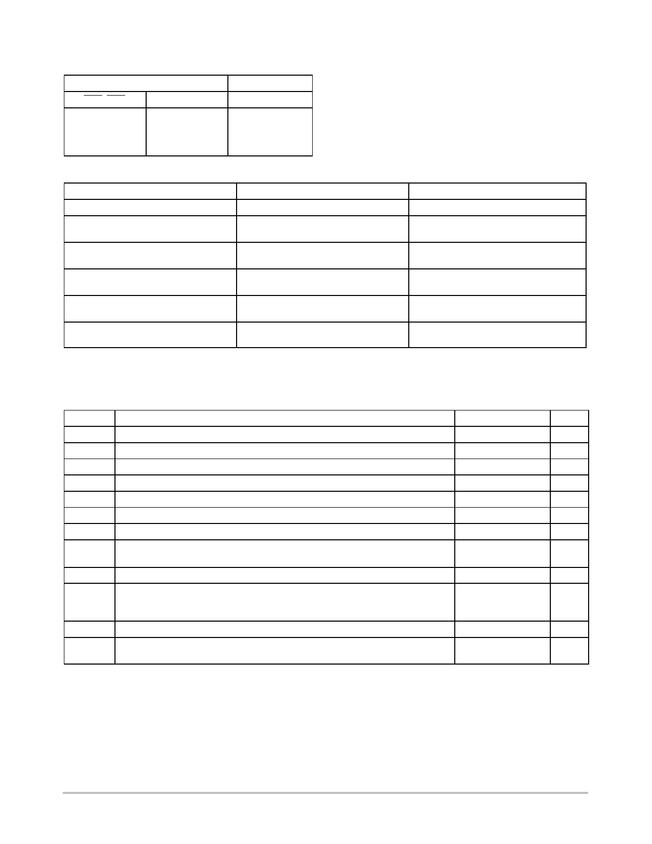
FUNCTION TABLE
INPUTS
OEA, OEB
A, B
L
L
L
H
H
X
OUTPUTS
YA, YB
L
H
Z
ORDERING INFORMATION
Device
Package
Shipping†
MC74VHC244DW − OBSOLETE*
SOIC−20 WB
38 Units/Rail
MC74VHC244DWR2G
SOIC−20 WB
(Pb−Free)
1000/Tape & Reel
MC74VHC244DTG
TSSOP−20
(Pb−Free)
75 Units/Rail
MC74VHC244DTR2G
TSSOP−20
(Pb−Free)
2500/Tape & Reel
MC74VHC244M − OBSOLETE*
SOIC EIAJ−20
(Pb−Free)
1600 Units/Box
MC74VHC244MELG
SOIC EIAJ−20
(Pb−Free)
2000/Tape & Reel
*This device is obsolete, information available for reference.
†For information on tape and reel specifications, including part orientation and tape sizes, please refer to our Tape and Reel Packaging
Specifications Brochure, BRD8011/D.
MAXIMUM RATINGS (Note 1)
Symbol
Parameter
Value
Unit
VCC
VIN
VOUT
IIK
IOK
IOUT
ICC
PD
Positive DC Supply Voltage
Digital Input Voltage
DC Output Voltage
Input Diode Current
Output Diode Current
DC Output Current, per Pin
DC Supply Current, VCC and GND Pins
Power Dissipation in Still Air
−0.5 to +7.0
V
−0.5 to +7.0
V
−0.5 to VCC +0.5
V
−20
mA
$20
mA
$25
mA
$75
mA
SOIC
500
mW
TSSOP
450
TSTG
VESD
Storage Temperature Range
ESD Withstand Voltage
−65 to +150
°C
Human Body Model (Note 2)
>2000
V
Machine Model (Note 3)
>200
Charged Device Model (Note 4)
>2000
ILATCHUP Latchup Performance
Above VCC and Below GND at 125°C (Note 5)
$300
mA
qJA
Thermal Resistance, Junction−to−Ambient
SOIC
96
TSSOP
128
°C/W
Stresses exceeding Maximum Ratings may damage the device. Maximum Ratings are stress ratings only. Functional operation above the
Recommended Operating Conditions is not implied. Extended exposure to stresses above the Recommended Operating Conditions may affect
device reliability.
1. Vin and Vout should be constrained to the range GND v (Vin or Vout) v VCC. Unused inputs must always be tied to an appropriate logic voltage
level (e.g., either GND or VCC). Unused outputs must be left open.
2. Tested to EIA/JESD22−A114−A
3. Tested to EIA/JESD22−A115−A
4. Tested to JESD22−C101−A
5. Tested to EIA/JESD78
http://onsemi.com
2
Share Link: 