P4C164L-100CMB Ver la hoja de datos (PDF) - Semiconductor Corporation
Número de pieza
componentes Descripción
Lista de partido
P4C164L-100CMB Datasheet PDF : 16 Pages
| |||
P4C164
AC ELECTRICAL CHARACTERISTICS—READ CYCLE
(VCC = 5V ± 10%, All Temperature Ranges)(2)
-8
-10
-12
-15
-20
-25
-35
-45
-70
-100
Symbol Parameter Min Max Min Max Min Max Min Max Min Max Min Max Min Max Min Max Min Max Min Max Unit
tRC
Read Cycle
Time
8
10
12
15
20
25
35
45
70
100
ns
tAA
Address
Access Time
tAC
Chip Enable
Access Time
8
10
12
15
20
25
35
45
70
100 ns
8
10
12
15
20
25
35
45
70
100 ns
Output Hold
tOH from Address 3
3
3
3
3
3
3
3
3
3
ns
Change
tLZ
Chip Enable to
Output in Low Z
2
2
2
2
2
2
2
2
2
2
ns
Chip Disable
tHZ to Output in
High Z
5
6
7
8
8
10
15
20
35
45 ns
Output Enable
tOE Low to Data
Valid
5
6
7
9
10
13
18
20
35
45 ns
tOLZ
Output Enable
Low to Low Z
2
2
2
2
2
2
2
2
2
2
ns
tOHZ
Output Enable
High to High Z
5
6
7
9
9
12
15
20
35
45 ns
Chip Enable to
tPU Power Up
0
0
0
0
0
0
0
0
0
0
ns
Time
Chip Disable
tPD to Power Down
8
Time
10
12
15
20
20
20
25
35
45 ns
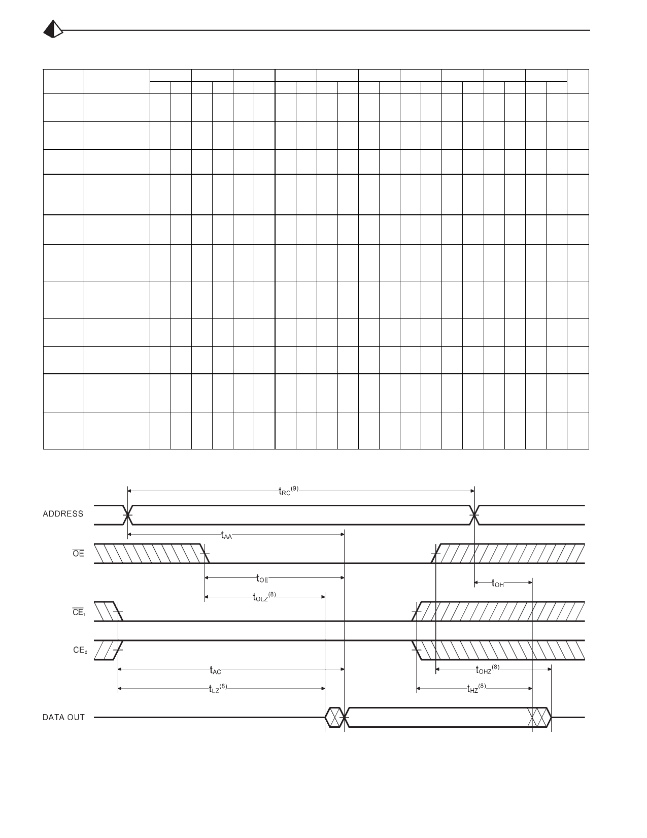
TIMING WAVEFORM OF READ CYCLE NO. 1 (OE CONTROLLED)(5)
Notes:
5. WE is HIGH for READ cycle.
6.
CE
1
is
LOW,
CE2
is
HIGH
and
OE
is
LOW
for
READ
cycle.
7.
ADDRESS
must
be
valid
prior
to,
or
coincident
with
CE
1
transition
LOW and CE2 transition HIGH.
Document # SRAM115 REV F
8. Transition is measured ± 200 mV from steady state voltage prior to
change, with loading as specified in Figure 1. This parameter is
sampled and not 100% tested.
Page 4 of 16
Share Link: 