P4C164L-100CMB Ver la hoja de datos (PDF) - Semiconductor Corporation
Número de pieza
componentes Descripción
Lista de partido
P4C164L-100CMB Datasheet PDF : 16 Pages
| |||
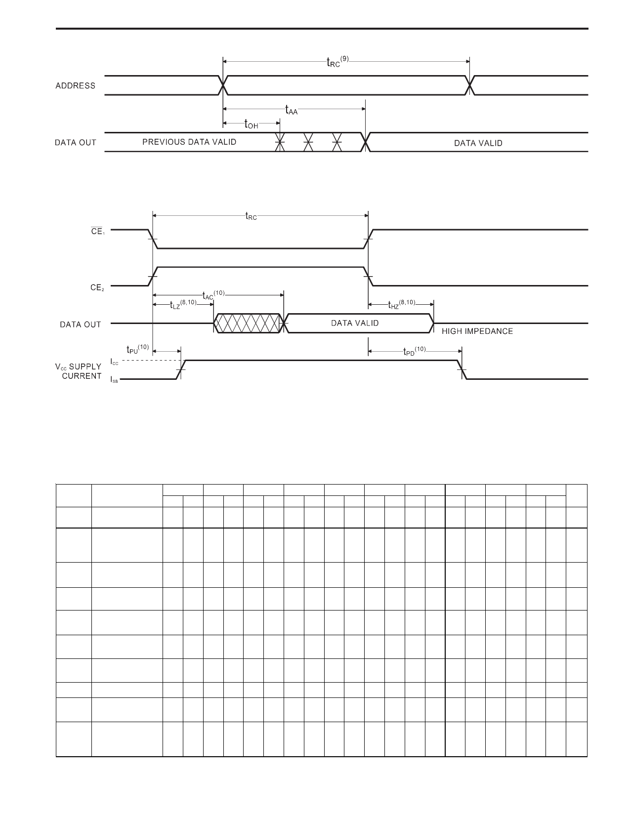
TIMINIG WAVERFORM OF READ CYCLE NO. 2 (ADDRESS CONTROLLED)(5,6)
P4C164
TIMING WAVEFORM OF READ CYCLE NO. 3 (CE1, CE2 CONTROLLED)(5,7,10)
Notes:
9. READ Cycle Time is measured from the last valid address to the first
transitioning address.
10. Transitions caused by a chip enable control have similar delays
irrespective
of
whether
CE
1
or
CE2
causes
them.
AC CHARACTERISTICS—WRITE CYCLE
(VCC = 5V ± 10%, All Temperature Ranges)(2)
-8
-10
-12
-15
-20
-25
-35
-45
-70
-100
Symbol Parameter Min Max Min Max Min Max Min Max Min Max Min Max Min Max Min Max Min Max Min Max Unit
tWC Write Cycle Time 8
10
12
15
20
25
35
45
70
100
ns
Chip Enable
tCW Time to End of 6
Write
tAW
Address Valid to
End of Write
7
tA S
Address Set-up
Time
0
tWP
Write Pulse
Width
7
tA H
Address Hold
Time
0
tDW
Data Valid to
End of Write
6
7
8
12
15
18
25
33
50
70
ns
8
10
12
15
18
25
33
50
70
ns
0
0
0
0
0
0
0
0
0
ns
8
9
12
15
18
20
25
40
50
ns
0
0
0
0
0
0
0
0
0
ns
7
8
9
11
13
15
20
30
40
ns
tDH Date Hold Time 0
0
0
0
0
0
0
0
0
0
ns
tWZ
Write Enable to
Output in High Z
6
7
7
7
8
10
14
18
30
40 ns
Output Active
tOW from End of
3
3
3
3
3
3
3
3
3
3
ns
Write
Document # SRAM115 REV F
Page 5 of 16
Share Link: 