RF2668 Ver la hoja de datos (PDF) - RF Micro Devices
Número de pieza
componentes Descripción
Lista de partido
RF2668 Datasheet PDF : 16 Pages
| |||
Preliminary
RF2668
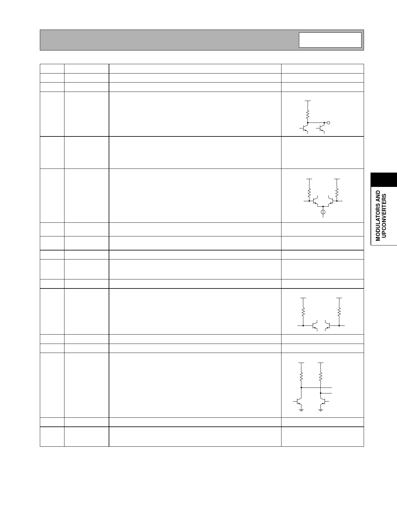
Pin Function Description
Interface Schematic
1
NC
Not connected.
2
NC
Not connected.
3
RF OUT RF output pin. An external shunt inductor to VCC plus a series blocking/
VCC4
matching capacitor are required for 50Ω output.
300 Ω
RF OUT
4
VCC4
Supply for the mixer stage only. The supply for the mixer is separated to
maximize IF to RF isolations and reduce the carrier leakage. A 10nF
external bypass capacitor is required. The trace length between the pin
and the bypass capacitors should be minimized. The ground side of the
bypass capacitors should connect immediately to ground plane.
5
LO2+
One half of the balanced mixer LO2 input. In single-ended applications,
the other half of the input, LO2- is AC grounded. This is a 50Ω imped-
BIAS
BIAS
5
ance port. This pin is NOT internally DC-blocked. An external blocking
capacitor (100pF recommended) must be provided if the pin is con-
nected to a device with DC present.
50 Ω
LO2+
50 Ω
LO2-
6
LO2-
One half of the balance mixer LO2 input. In single ended applications, See pin 5.
this pin is AC grounded with a 100pF capacitor.
7
GND2
Ground connection for the mixer stage. For best performance, keep
traces physically short and connect immediately to ground plane.
8
GND2
Same as pin 7.
9
MIX_DEC Current Mirror decoupling pin. A 1000pF external capacitor is required
to bypass this pin. The ground side of the bypass capacitors should
connect immediately to ground plane.
10
MIX IN+ Same as pin 11, except complementary input.
See pin 11.
11
MIX IN- One half of the 200Ω balanced impedance input to the mixer stage.
BIAS
This pin is NOT internally DC-blocked. An external blocking capacitor
(1000pF recommended) must be provided if the pin is connected to a
device with DC present. If no IF filter is needed this pin may be con-
100 Ω
nected to MOD OUT+ through a DC blocking capacitor. An appropriate
matching network may be needed if an IF filter is used.
MIX IN-
BIAS
100 Ω
MIX IN+
12
NC
Not connected.
13
NC
Not connected.
14
MOD OUT- One half of the balanced AGC output port. The impedance of this port
is 200Ω balanced. If no filtering is required, this pin can be connected
to the MIX IN- pin through a DC blocking capacitor. This pin requires an
inductor to VCC to achieve full dynamic range. In order to maximize
gain, this inductor should be a high-Q type and should be parallel reso-
nated out with a capacitor (see application schematic). This pin is NOT
DC-blocked. A blocking capacitor of 2200pF is needed when this pin is
connected to a DC path. An appropriate matching network may be
needed if an IF filter is used.
VCC3
VCC3
100 Ω
100 Ω
MOD OUT-
MOD OUT+
15 MOD OUT+ Same as pin 14, except complementary output.
See pin 14.
16
GND1
Ground connection for all baseband circuits including bandgap, AGC,
flip-flop, modulator and FM amp. For best performance, keep traces
physically short and connect immediately to ground plane.
Rev B4 010423
5-75
Share Link: 