RF2668 Ver la hoja de datos (PDF) - RF Micro Devices
Número de pieza
componentes Descripción
Lista de partido
RF2668 Datasheet PDF : 16 Pages
| |||
Preliminary
RF2668
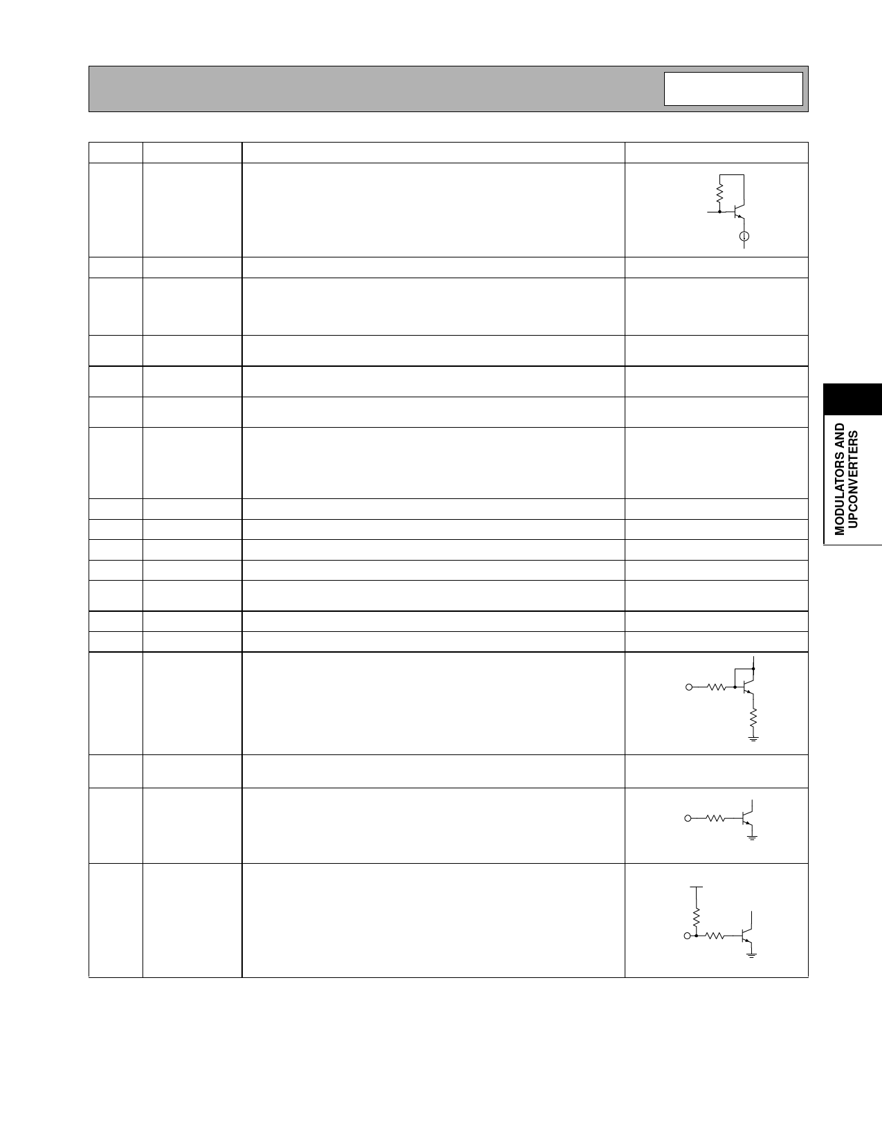
Pin Function Description
Interface Schematic
29
LO1+
External LO input to modulator. Controlled by VCO_EN signal. Logic
low is internal VCO, while logic high is external VCO.
1 kΩ
LO1+, FM+
30
VCO-
See VCO+ description.
31
VCO+
This port is used to supply DC voltage to the VCO as well as to tune the
center frequency of the VCO. Equal value inductors should be con-
nected to this pin and pin 30 although a small imbalance can be used
to tune in the proper frequency range.
32
DO
Output of the charge pump, and input to the VCO control. An RC net-
work from this pin to ground is used to establish the PLL bandwidth.
33
LD
Lock detector output for synthesizer. Requires external transistor to
provide hysteresis and inversion of signal. See Application circuit.
34
PLLGND Ground for synthesizer. For best performance, keep traces physically
5
short and connect immediately to ground plane.
35
PLLVCC Supply for the PLLVCC only. A 10nF external bypass capacitor is
required and an additional 0.1µF will be required if no other low fre-
quency bypass capacitors are nearby. The trace length between the pin
and the bypass capacitors should be minimized. The ground side of the
bypass capacitors should connect immediately to ground plane.
36
SET2
PLL Setting (Divider) pin. See the PLL settings table.
37
SET1
Same as pin 36.
38
OSCREF TCXO reference input for synthesizer.
39
VREFPLL Bypass pin for the synthesizer reference voltage.
40
PLLISET Current setting pin for synthesizer charge pump. For normal operation,
a 390Ω resistor to ground should be used to set the current.
41
PLLON Synthesizer Enable pin.
See pin 45.
42
VCO_EN VCO Enable pin. Switches between internal and external VCO.
See pin 45.
43
MIX_EN Power down control for mixer only. When connected to logic “high”
(>VCC-0.3) the mixer circuits are operating; when connected to ground
(≤0.3V), the mixer is turned off but all other circuits are operating. A DC
MIX EN
1 kΩ
voltage less than or equal to the maximum allowable VCC may be
applied to this pin when no voltage is applied to the VCC pins.
450 Ω
44
TX_EN
Shuts down the entire TX path. VCO is still active when TX disabled.
Logic high (>VCC -0.3) for TX Enable.
45
CE
Power down control for overall circuit. When logic “high” (≥VCC -0.3V),
all circuits are operating; when logic “low” (≤0.3V), all circuits are
10 kΩ
CE
turned off. The input impedance of this pin is >10kΩ. A DC voltage less
than or equal to the maximum allowable Vcc may be applied to this pin
when no voltage is applied to the VCC pins.
46
MODE
Selects between CDMA and FM mode. This is a digitally controlled
input. A logic “high” (≥VCC -0.3VDC) selects CDMA mode. A logic “low”
BIAS
(<0.3VDC) selects FM mode. In FM mode, this switch enables the FM
amplifier and turns off the I&Q modulator. The impedance on this pin is
60 kΩ
30kΩ. A DC voltage less than or equal to the maximum allowable VCC
may be applied to this pin when no voltage is applied to the VCC pins.
MODE
60 kΩ
Rev B4 010423
5-77
Share Link: 