RF2668 Ver la hoja de datos (PDF) - RF Micro Devices
Número de pieza
componentes Descripción
Lista de partido
RF2668 Datasheet PDF : 16 Pages
| |||
RF2668
Preliminary
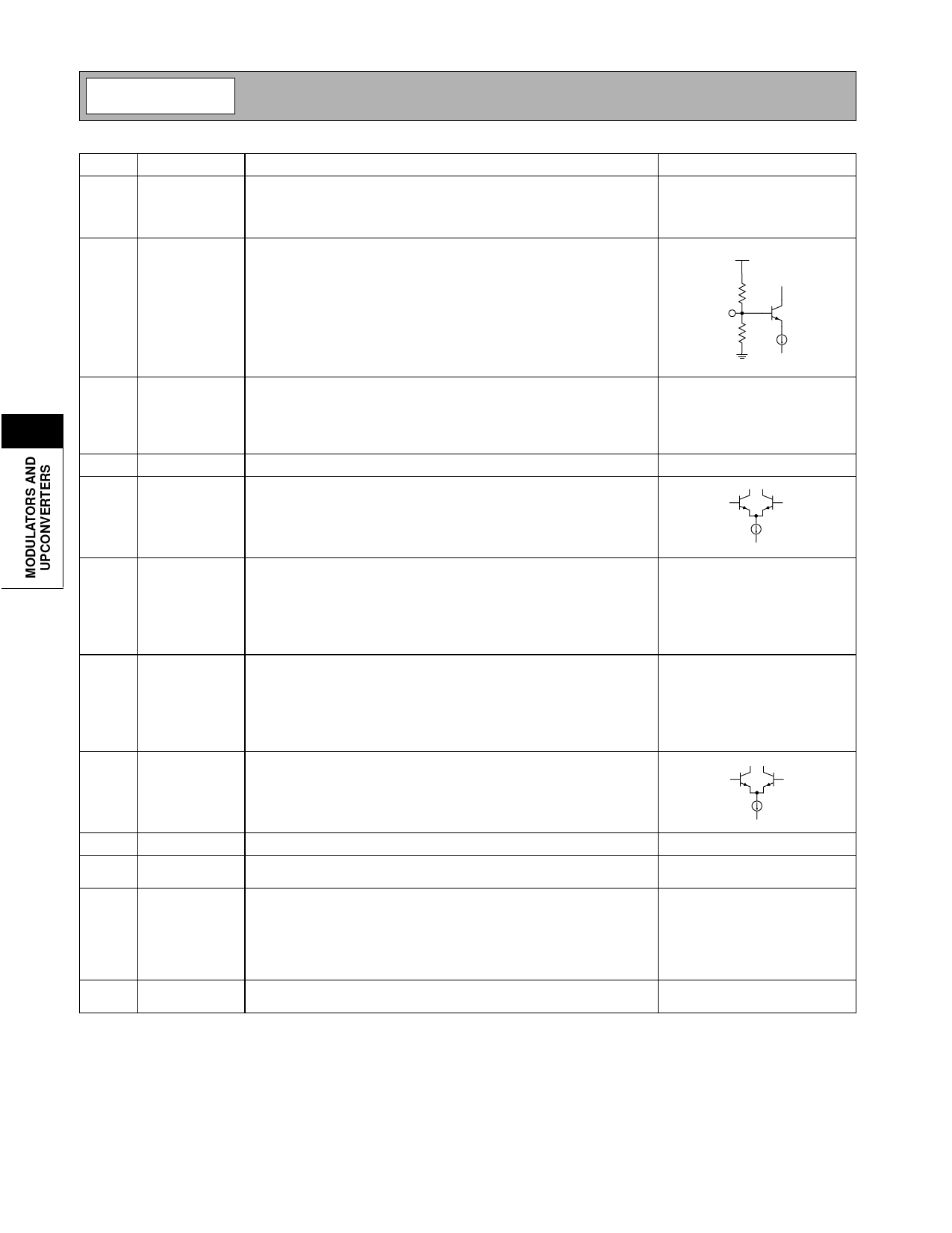
Pin Function Description
Interface Schematic
17
AGC_DEC AGC decoupling pin. An external bypass capacitor of 1nF capacitor is
required. The trace length between the pin and the bypass capacitors
should be minimized. The ground side of the bypass capacitors should
connect immediately to ground plane.
18
VGC
Analog gain control for AGC amplifiers. Valid control voltage ranges are
from 0.3VDC to 2.4VDC. The gain range for the AGC is 95dB. These
voltages are valid ONLY for a 39kΩ source impedance. A DC voltage
less than or equal to the maximum allowable VCC may be applied to
this pin when no voltage is applied to the VCC pins.
BIAS
21 kΩ
GC
40 kΩ
19
VCC2
Supply for the modulator stage only. A 10nF external bypass capacitor
is required and an additional 0.1µF will be required if no other low fre-
quency bypass capacitors are nearby. The trace length between the pin
5
and the bypass capacitors should be minimized. The ground side of the
bypass capacitors should connect immediately to ground plane.
20
GND1
Same as pin 16.
21
Q SIG
Baseband input to the Q mixer. This pin is DC-coupled. The DC level of
1.3V must be supplied to this pin to bias the transistor. Input imped-
Q SIG
ance of this pin is 50kΩ minimum. A DC voltage less than or equal to
the maximum allowable VCC may be applied to this pin when no voltage
is applied to the VCC pins.
22
Q REF
Reference voltage for the Q mixer. This voltage should be the same as See pin 21.
the DC voltage supplied to the Q SIG pin. For maximum carrier sup-
pression, DC voltage on this pin relative to the Q SIG DC voltage may
be adjusted. Input impedance of this pin is 50kΩ minimum. A DC volt-
age less than or equal to the maximum allowable VCC may be applied
to this pin when no voltage is applied to the VCC pins.
23
I REF
Reference voltage for the I mixer. This voltage should be the same as See pin 24.
the DC voltage supplied to the I SIG pin. For maximum carrier suppres-
sion, DC voltage on this pin relative to the I SIG DC voltage may be
adjusted. Input impedance of this pin is 50kΩ minimum. A DC voltage
less than or equal to the maximum allowable VCC may be applied to
this pin when no voltage is applied to the VCC pins.
24
I SIG
Baseband input to the I mixer. This pin is DC coupled. The DC level of
1.3V must be supplied to this pin to bias the transistor. Input imped-
I SIG
ance of this pin is 50kΩ minimum. A DC voltage less than or equal to
the maximum allowable VCC may be applied to this pin when no voltage
is applied to the VCC pins.
25
NC
Not connected.
Q REF
I REF
26 VCO_ISET An external resistor of 47kΩ is used to set the VCO current for mini-
mum phase noise.
27
VCC1
Supply Voltage for the LO1 flip-flop and limiting amp only. This supply is
isolated to minimize the carrier leakage. A 1nF external bypass capaci-
tor is required, and an additional 0.1µF will be required if no other low
frequency bypass capacitors are nearby. The trace length between the
pin and the bypass capacitors should be minimized. The ground side of
the bypass capacitors should connect immediately to ground plane.
28
LO1-
External LO input to modulator. Controlled by VCO_EN signal. Logic See pin 29.
low is internal VCO, while logic high is external VCO.
5-76
Rev B4 010423
Share Link: 