CS5317 Ver la hoja de datos (PDF) - Cirrus Logic
Número de pieza
componentes Descripción
Lista de partido
CS5317 Datasheet PDF : 32 Pages
| |||
CS5317
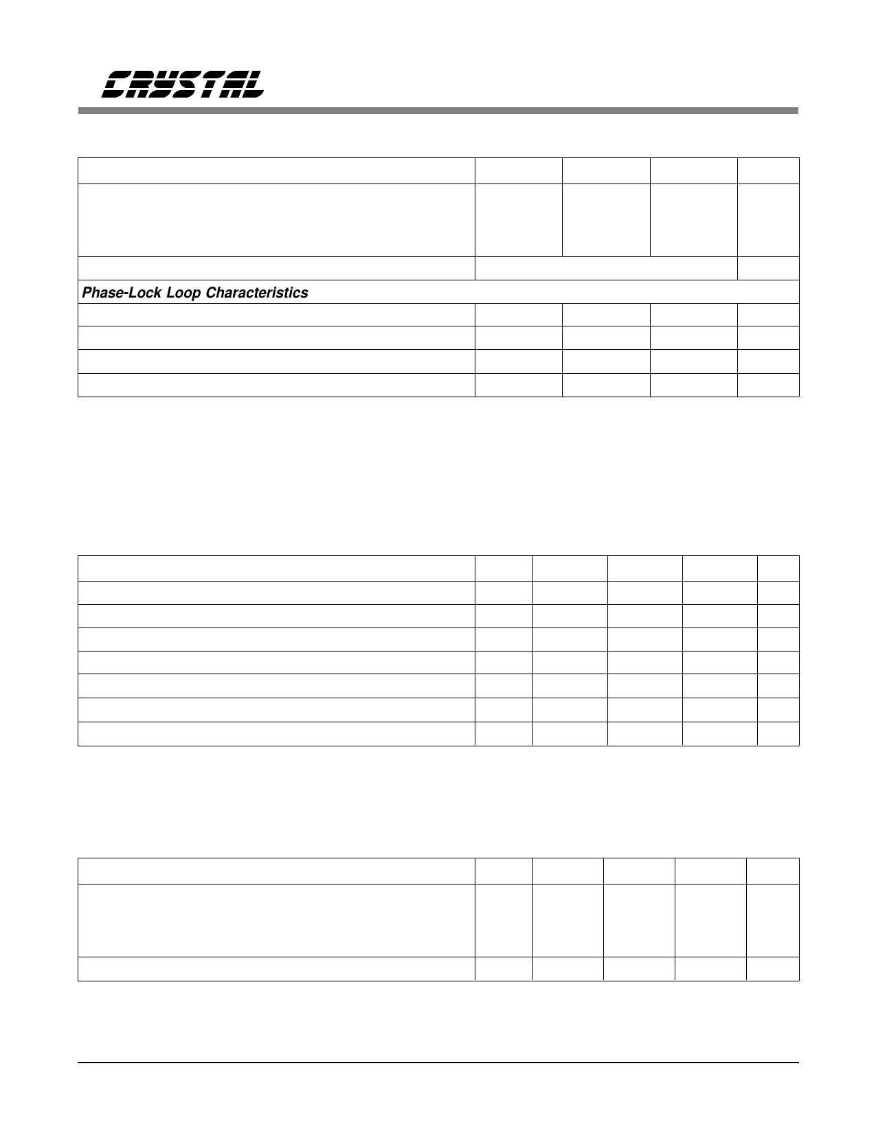
ANALOG CHARACTERISTICS (continued)
Parameter
Min
Typ
Max
Power Supply Rejection
VA+
VA-
VD+
VD-
(Note 6)
-
60
-
-
45
-
-
60
-
-
55
-
Specified Temperature Range
0 to 70
Phase-Lock Loop Characteristics
VCO Gain Constant, Ko
(Note 7)
-4
-10
-30
VCO Operating Frequency
1.28
-
5.12
Phase Detector Gain Control, Kd
-3
-8
-12
Phase Detector Prop. Delay
(Note 8)
-
50
100
Notes: 6. With 300mV p-p, 1kHz ripple applied to each supply separately.
7. Over 1.28 MHz to 5.12 MHz VCO output range, where VCO frequency = 2 * CLKOUT.
8. Delay from an input edge to the phase detector to a response at the PHDT output pin.
Units
dB
dB
dB
dB
°C
Mrad/Vs
MHz
µA/rad
ns
DIGITAL CHARACTERISTICS (TA = TMIN - TMAX; VA+, VD+ = 5V±10%; VA-, VD- = -5V±10%)
All measurements performed under static conditions.
Parameter
Symbol Min
Typ
Max Units
High-Level Input Voltage
VIH
2.0
-
-
V
Low-Level Input Voltage
VIL
-
-
0.8
V
High-Level Output Voltage
(Note 9) VOH (VD+)-1.0V
-
-
V
Low-Level Output Voltage IOUT = 1.6mA
VOL
-
-
0.4
V
Input Leakage Current
Iin
-
-
10
µA
3-State Leakage Current
IOZ
-
-
±10
µA
Digital Output Pin Capacitance
Cout
-
9
-
pF
Note: 9. Iout=-100µA. This specification guarantees the ability to drive one TTL load (VOH=2.4V @ Iout=-40µA.).
RECOMMENDED OPERATING CONDITIONS (DGND, AGND = 0V, see Note 10.)
Parameter
Symbol Min
Typ
Max
DC Power Supplies:
Positive Digital
Negative Digital
Positive Analog
Negative Analog
Master Clock Frequency
Note: 10. All voltages with respect to ground.
VD+
4.5
5.0
5.5
VD-
-4.5
-5.0
-5.5
VA+
4.5
5.0
5.5
VA-
-4.5
-5.0
-5.5
fclk
0.01
-
5.12
Specifications are subject to change without notice.
Units
V
V
V
V
MHz
DS27F4
3
Share Link: 