FM25C160B-GA(2014) Ver la hoja de datos (PDF) - Cypress Semiconductor
Número de pieza
componentes Descripción
Lista de partido
FM25C160B-GA Datasheet PDF : 20 Pages
| |||
FM25C160B
SPI Modes
FM25C160B may be driven by a microcontroller with its SPI
peripheral running in either of the following two modes:
■ SPI Mode 0 (CPOL = 0, CPHA = 0)
■ SPI Mode 3 (CPOL = 1, CPHA = 1)
For both these modes, the input data is latched in on the rising
edge of SCK starting from the first rising edge after CS goes
active. If the clock starts from a HIGH state (in mode 3), the first
rising edge after the clock toggles is considered. The output data
is available on the falling edge of SCK.
The two SPI modes are shown in Figure 4 on page 6 and Figure
5 on page 6. The status of the clock when the bus master is not
transferring data is:
■ SCK remains at 0 for Mode 0
■ SCK remains at 1 for Mode 3
The device detects the SPI mode from the status of the SCK pin
when the device is selected by bringing the CS pin LOW. If the
SCK pin is LOW when the device is selected, SPI Mode 0 is
assumed and if the SCK pin is HIGH, it works in SPI Mode 3.
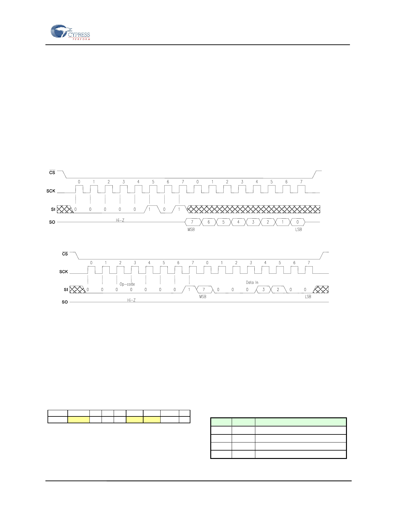
Figure 4. SPI Mode 0
CS
SCK
0 1 234 56 7
Table 1. Opcode commands
Name
WREN
WRDI
RDSR
WRSR
READ
WRITE
Description
Set write enable latch
Write disable
Read Status Register
Write Status Register
Read memory data
Write memory data
Opcode
0000 0110b
0000 0100b
0000 0101b
0000 0001b
0000 0011b
0000 0010b
WREN - Set Write Enable Latch
The FM25C160B will power up with writes disabled. The WREN
command must be issued before any write operation. Sending
the WREN opcode allows the user to issue subsequent opcodes
for write operations. These include writing the Status Register
(WRSR) and writing the memory (WRITE).
Sending the WREN opcode causes the internal Write Enable
Latch to be set. A flag bit in the Status Register, called WEL,
indicates the state of the latch. WEL = ‘1’ indicates that writes are
permitted. Attempting to write the WEL bit in the Status Register
has no effect on the state of this bit – only the WREN opcode can
set this bit. The WEL bit will be automatically cleared on the rising
edge of CS following a WRDI, a WRSR, or a WRITE operation.
This prevents further writes to the Status Register or the F-RAM
array without another WREN command. Figure 6 illustrates the
WREN command bus configuration.
Figure 6. WREN Bus Configuration
SI
7 6543210
MSB
LSB
CS
SCK
01 234567
Figure 5. SPI Mode 3
CS
SCK
0 1 234 56 7
SI
7 654321 0
MSB
LSB
Power Up to First Access
The FM25C160B is not accessible for a tPU time after power up.
Users must comply with the timing parameter tPU, which is the
minimum time from VDD (min) to the first CS LOW.
Command Structure
There are six commands, called opcodes, that can be issued by
the bus master to the FM25C160B. They are listed in Table 1.
These opcodes control the functions performed by the memory.
SI
00000110
SO
HI-Z
WRDI - Reset Write Enable Latch
The WRDI command disables all write activity by clearing the
Write Enable Latch. The user can verify that writes are disabled
by reading the WEL bit in the Status Register and verifying that
WEL is equal to ‘0’. Figure 7 illustrates the WRDI command bus
configuration.
Figure 7. WRDI Bus Configuration
CS
SCK
01 234567
SI
0000 0 10 0
SO
HI-Z
Document Number: 001-86150 Rev. *A
Page 6 of 20
Share Link: 