RMWB11001 Ver la hoja de datos (PDF) - Fairchild Semiconductor
Número de pieza
componentes Descripción
Lista de partido
RMWB11001 Datasheet PDF : 6 Pages
| |||
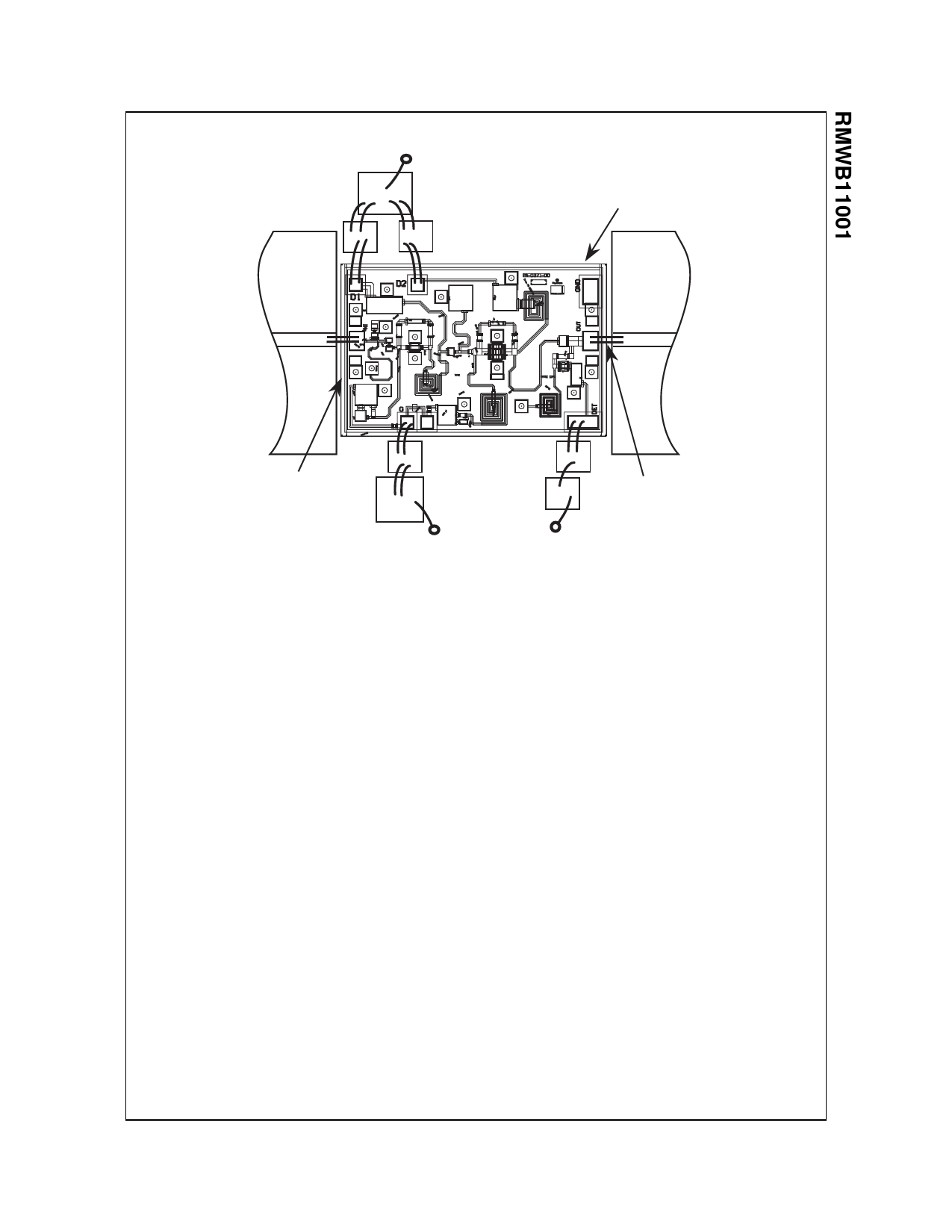
Figure 3. Recommended Assembly Diagram
10,000pF
100pF
Vd
(Positive)
100pF
Die-Attach
80Au/20Sn
5mil Thick
Alumina
50Ω
5 mil Thick
Alumina
50Ω
RF
Input
RF
Output
2 mil Gap
100pF
100pF
10,000pF
3KΩ
Vg (Negative)
L< 0.015”
(4 Places)
Vdet (Positive)
Notes:
Use 0.003" by 0.0005" Gold Ribbon for bonding.RF input and output bonds should be less than 0.015" long with stress relief. Detector delivers approx. 0.5V DC into
3 kΩ load resistor for >+18 dBm output power. If output power level detection is not desired do not make connection to detector bond pad.
Application Information
CAUTION: THIS IS AN ESD SENSITIVE DEVICE.
Chip carrier material should be selected to have GaAs
compatible thermal coefficient of expansion and high
thermal conductivity such as copper molybdenum or copper
tungsten. The chip carrier should be machined, finished flat,
plated with gold over nickel and should be capable of
withstanding 325°C for 15 minutes.
Die attachment should utilize Gold/Tin (80/20) eutectic alloy
solder and should avoid hydrogen environment for PHEMT
devices. Note that the backside of the chip is gold plated
and is used as RF and DC ground.
These GaAs devices should be handled with care and
stored in dry nitrogen environment to prevent contamination
of bonding surfaces. These are ESD sensitive devices and
should be handled with appropriate precaution including the
use of wrist grounding straps. All die attach and wire/ribbon
bond equipment must be well grounded to prevent static
discharges through the device.
Recommended wire bonding uses 3 mils wide and 0.5 mil
thick gold ribbon with lengths as short as practical allowing
for appropriate stress relief. The RF input and output bonds
should be typically 0.012" long corresponding to a typical 2
mil gap between the chip and the substrate material.
Recommended Procedure for Biasing and Operation
CAUTION: LOSS OF GATE VOLTAGE (Vg) WHILE
DRAIN VOLTAGE (Vd) IS PRESENT MAY DAMAGE THE
AMPLIFIER CHIP.
The following sequence of steps must be followed to
properly test the amplifier:
Step 1: Turn off RF input power.
Step 2: Connect the DC supply grounds to the ground of
the chip carrier. Slowly apply negative gate bias
supply voltage of -1.5V to Vg.
Step 3: Slowly apply positive drain bias supply voltage of
+4V to Vd.
Step 4: Adjust gate bias voltage to set the quiescent
current of Idq = 36mA.
Step 5: After the bias condition is established, the RF input
signal may now be applied at the appropriate
frequency band.
Step 6: Follow turn-off sequence of:
(i) Turn off RF input power,
(ii) Turn down and off drain voltage (Vd),
(iii) Turn down and off gate bias voltage (Vg).
©2004 Fairchild Semiconductor Corporation
RMWB11001 Rev. C
Share Link: 