LT1680 Ver la hoja de datos (PDF) - Linear Technology
Número de pieza
componentes Descripción
Lista de partido
LT1680 Datasheet PDF : 16 Pages
| |||
LT1680
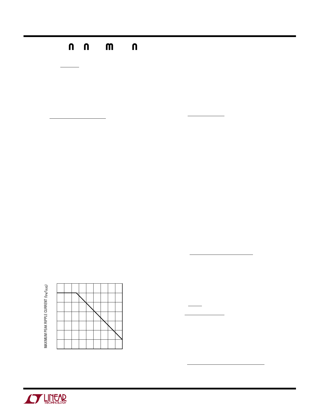
APPLICATIONS INFORMATION
SX
=
0.084
fO
RSENSE
Amp/s
where fO is oscillator frequency and RSENSE is the external
current sense resistor. This yields a minimum inductance
requirement of:
[ ] LMIN
≥
(VIN)(RSENSE)(2DC –1)
(0.084)(fO)(1− DC)
A down side of slope compensation is that, since the IC
servo loop senses an increase in perceived inductor cur-
rent, the internal current limit functions are affected such
that the maximum current capability of a regulator is
reduced by the same amount as the effective current
referred slope compensation. The LT1680, however, uses
a current limit scheme that is independent of the slope
compensation effects (Average Current Limiting). This
provides operation at any duty cycle with no reduction in
current sourcing capability, provided ripple current peak
amplitude is less than 15% of the current limit value. For
example, if the converter is set up to average current limit
at 10A, as long as the peak inductor current is less than
11.5A, duty cycles up to 90% can be achieved without
compromising the average current limit value.
If an inductor smaller than the minimum required for
internal slope compensation (calculated above as LMIN) is
desired, additional slope compensation is necessary. The
LT1680 provides this capability through the SL/ADJ pin.
1.45
1.40
1.35
1.30
1.25
1.20
1.15
1.10
0 0.1 0.2 0.3 0.4 0.5 0.6 0.7 0.8 0.9
DUTY CYCLE
1680 F10
Figure 10. Maximum Peak Ripple Current (Normalized)
vs Duty Cycle for Average Current Limit
This feature is implemented by referencing this pin via a
resistor divider from the 5VREF pin to ground. The addi-
tional slope compensation will be affected at the point in
the oscillator waveform (at pin CT) corresponding to the
voltage set by the resistor divider. Additional slope com-
pensation can be calculated using the relation:
( ( )( )( ) ) SX =
2500 fO
RTH RSENSE
Amp/s
where RTH is the Thevenin resistance of the resistor
divider. Actual compensation will actually be somewhat
greater due to internal curvature correction circuitry that
imposes an exponential increase in the slope compensa-
tion waveform, further increasing the effective compensa-
tion slope up to 20% for a given setting.
Design example:
VIN = 20V
VOUT = 80V (DC = 0.75)
RSENSE = 0.01Ω
fO = 100kHz
L = 20µH
The minimum inductor usable with no additional slope
compensation is:
LMIN
≥
(20V)(0.01Ω)(1.5 – 1)
(0.084)(100000)(1– 0.75)
=
47.6µH
Since L = 20µH is less than LMIN, additional slope
compensation is necessary. The total slope compensa-
tion required is:
SX
≥
20V
20µH
(1.5
1– 0.75
–
1)
=
(2)(106 )
Amp/s
Subtracting the internally generated slope compensation
and solving for the required effective resistance at SL/ADJ
yields:
( ) ( ( )() )( )( ) REQ ≤
2500 fO
2
106
RSENSE
–
0.084
fO
= 21.5k
13
Share Link: 