LT1680 Ver la hoja de datos (PDF) - Linear Technology
Número de pieza
componentes Descripción
Lista de partido
LT1680 Datasheet PDF : 16 Pages
| |||
LT1680
APPLICATIONS INFORMATION
The input bypass capacitors generally have less ripple
current than the output bypass capacitors as the input
current in a boost converter is continuous. Input bypass
capacitor selection can be made using ripple current
ratings. Peak-to-peak ripple current is equal to the induc-
tor ripple current (∆IL).
Efficiency Considerations and Heat Dissipation
High output power applications create an inherent con-
cern regarding power dissipation in regulator compo-
nents. Although high efficiencies are achieved using the
LT1680, the power dissipated in the regulator climbs to
relatively high values when the load draws large amounts
of power. Even at 90% efficiency, a 500W application has
conversion loss of 55W.
I2R dissipation in the MOSFET switch, sense resistor and
inductor series resistance can generate substantial con-
version loss under high current conditions. Generally, the
dominant I2R loss is evidenced in the FET switch, which is
proportional to the steady-state duty cycle, or conduction
time of the switch. For example, in a 5V to 48V boost
converter, the duty cycle is:
DC = 1 – (VIN/ VOUT)
DC = 1 – 5/48 ≈ 90%
The FET switch conducts inductor current for almost 90%
of the cycle time, and thus may require increased consid-
eration for dissipating I2R power.
Gate Drive Buffer
The LT1680 is designed to drive relatively large capacitive
loads. However, in certain applications, efficiency im-
provements can be realized by adding an external buffer
stage to drive the gate of the FET switch. When the switch
gate loads the driver output such that rise/fall times
exceed 100ns, buffers can sometimes result in efficiency
gains. Buffers can also reduce effects of back injection into
the gate driver output due to coupling of switch node
transitions through the switch FET CMILLER.
Optimizing Transient Response–
Compensation Component Values
The dominant compensation point for an LT1680 con-
verter is the VC pin (Pin 5), or error amplifier output. This
pin connects to an external series RC network, RVC and
CVC. The infinite permutations of input/output filtering,
capacitor ESR, input voltage, load current, etc. make for an
empirical method of optimizing loop response for a spe-
cific set of conditions.
Loop response can be observed by injecting a step change
in load current. This can be achieved by using a switchable
load. With the load switching, the transient response of the
output voltage can be observed with an oscilloscope.
Iterating through RC combinations will yield optimized
response. Refer to Application Note 19 in the 1990 Linear
Applications Handbook, Volume 1 for more information.
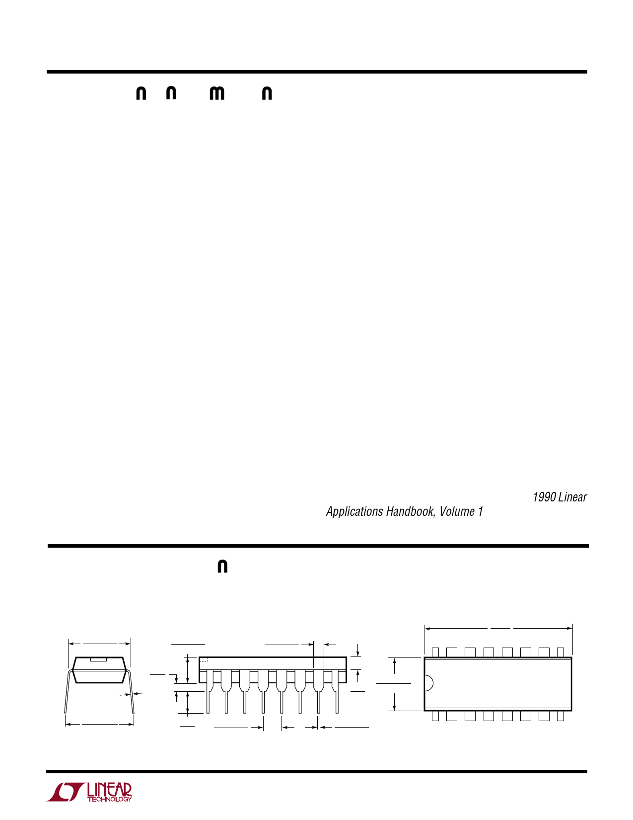
PACKAGE DESCRIPTION Dimensions in inches (millimeters) unless otherwise noted.
N Package
16-Lead PDIP (Narrow 0.300)
(LTC DWG # 05-08-1510)
0.300 – 0.325
(7.620 – 8.255)
0.130 ± 0.005
(3.302 ± 0.127)
0.045 – 0.065
(1.143 – 1.651)
0.009 – 0.015
(0.229 – 0.381)
0.020
(0.508)
MIN
+0.035
0.325 –0.015
( ) 8.255
+0.889
–0.381
0.125
(3.175)
MIN
0.100 ± 0.010
(2.540 ± 0.254)
*THESE DIMENSIONS DO NOT INCLUDE MOLD FLASH OR PROTRUSIONS.
MOLD FLASH OR PROTRUSIONS SHALL NOT EXCEED 0.010 INCH (0.254mm)
0.065
(1.651)
TYP
0.255 ± 0.015*
(6.477 ± 0.381)
0.018 ± 0.003
(0.457 ± 0.076)
0.770*
(19.558)
MAX
16 15 14 13 12 11 10 9
12
3
4
5
6
78
N16 1197
Information furnished by Linear Technology Corporation is believed to be accurate and reliable.
However, no responsibility is assumed for its use. Linear Technology Corporation makes no represen-
tation that the interconnection of its circuits as described herein will not infringe on existing patent rights.
15
Share Link: 