MX98L715BEC Ver la hoja de datos (PDF) - Macronix International
Número de pieza
componentes Descripción
Lista de partido
MX98L715BEC Datasheet PDF : 50 Pages
| |||
MX98L715BEC
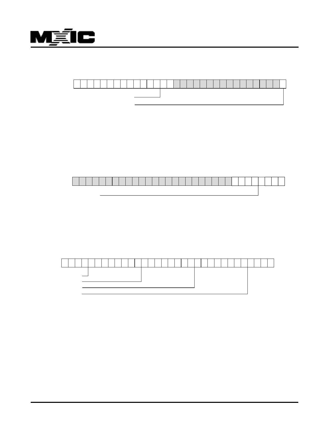
5.1.8 PCI BASE EXPANSION ROM ADDRESS REGISTER ( PBER ) ( Offset 33h-30h )
31 30 29 28 27 26 25 24 23 22 21 20 19 18 17 16 15 14 13 12 11 10 9 8 7 6 5 4 3 2 1 0
Expansion ROM Base Address (upper 21 bit)
Address Decode Enable
bit 0 : Address Decode Enable, decoding will be enabled if only both enable bit in PFCS<1> and this expansion ROM
register are 1.
bit 16 - 1 : not use
bit 31 - 17 : Defines the upper 21 bits of expansion ROM base address.
5.1.9 PCI CAPABILITY POINTER REGISTER ( PFCP ) ( Offset 37h-34h )
31 30 29 28 27 26 25 24 23 22 21 20 19 18 17 16 15 14 13 12 11 10 9 8 7 6 5 4 3 2 1 0
Capability Pointer (Set to 44h)
bit 7- 0 : Capability pointer (Cap_Ptr) is set to 44h.
bit 31- 8 : reserved
5.1.10 INTERRUPT REGISTER ( PFIT ) ( Offset 3Fh-3Ch )
31 30 29 28 27 26 25 24 23 22 21 20 19 18 17 16 15 14 13 12 11 10 9 8 7 6 5 4 3 2 1 0
0 0111 000 000 01 00 0
Max_Lat
Min-Gnt
Interrupt Pin
Interrupt Line
bit 7 - 0 : Interrupt Line, system BIOS will writes the routing information into this field, driver can use this information
to determine priority and interrupt vector.
bit 15 - 8 : Interrupt Pin, fixed to 01h which use INTA#.
bit 31 - 24 : Max_Lat which is a maximum period for a access to PCI bus.
bit 23 - 16 : Min_Gnt which is the maximum period that MX98L715BEC needs to finish a burst PCI cycle.
P/N:PM0695
REV. 0.3, MAR. 30, 2001
11
Share Link: 