82C55A_15 Ver la hoja de datos (PDF) - Intersil
Número de pieza
componentes Descripción
Lista de partido
82C55A_15 Datasheet PDF : 30 Pages
| |||
82C55A
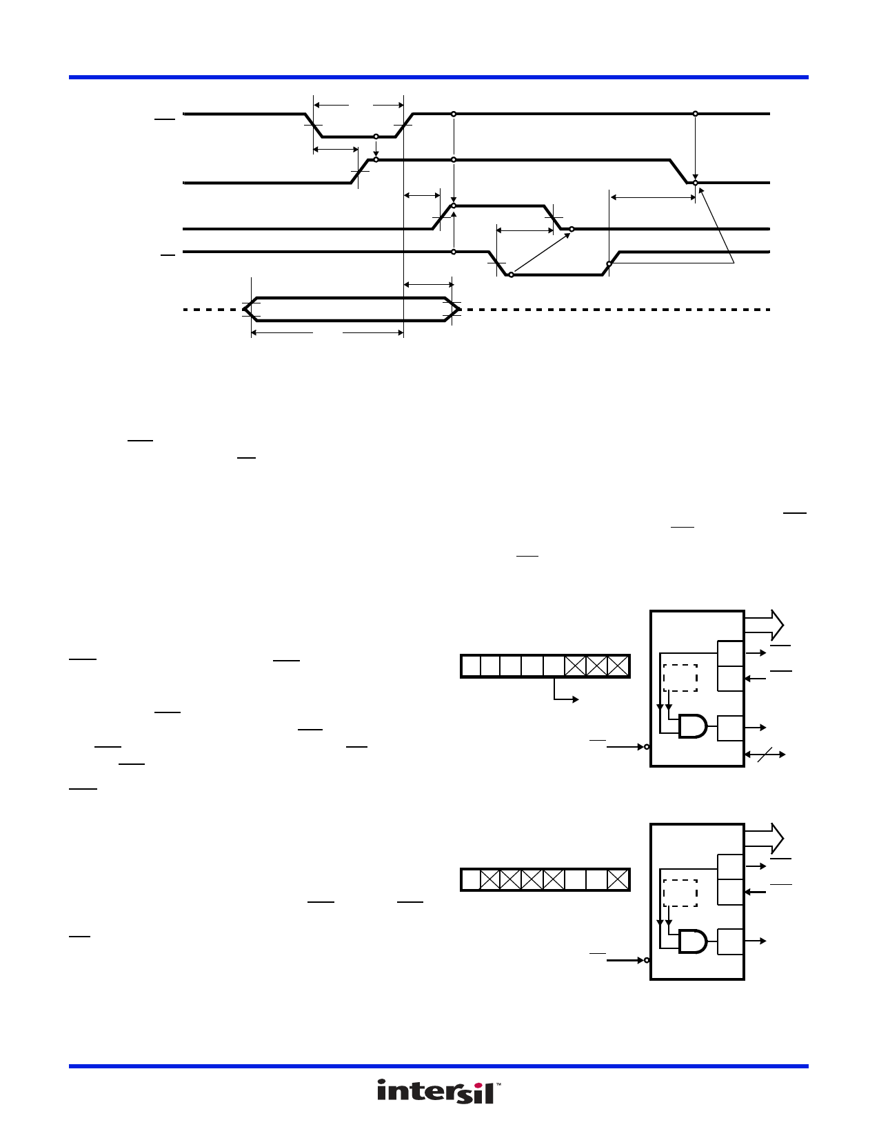
STB
IBF
INTR
tST
tSIB
tSIT
tRIT
tRIB
RD
INPUT FROM
PERIPHERAL
tPH
tPS
FIGURE 7. MODE 1 (STROBED INPUT)
INTR (Interrupt Request)
A “high” on this output can be used to interrupt the CPU when
an input device is requesting service. INTR is set by the
condition: STB is a “one”, IBF is a “one” and INTE is a “one”. It
is reset by the falling edge of RD. This procedure allows an
input device to request service from the CPU by simply
strobing its data into the port.
INTE A
Controlled by bit set/reset of PC4.
INTE B
Controlled by bit set/reset of PC2.
Output Control Signal Definition
(Figure 8 and 9)
OBF - (Output Buffer Full F/F). The OBF output will go “low”
to indicate that the CPU has written data out to the specified
port. This does not mean valid data is sent out of the port at
this time since OBF can go true before data is available. Data
is guaranteed valid at the rising edge of OBF, (See Note 1).
The OBF F/F will be set by the rising edge of the WR input and
reset by ACK input being low.
ACK - (Acknowledge Input). A “low” on this input informs the
82C55A that the data from Port A or Port B is ready to be
accepted. In essence, a response from the peripheral device
indicating that it is ready to accept data, (See Note 1).
INTR - (Interrupt Request). A “high” on this output can be used
to interrupt the CPU when an output device has accepted data
transmitted by the CPU. INTR is set when ACK is a “one”, OBF
is a “one” and INTE is a “one”. It is reset by the falling edge of
WR.
INTE A
Controlled by Bit Set/Reset of PC6.
INTE B
Controlled by Bit Set/Reset of PC2.
NOTE:
1. To strobe data into the peripheral device, the user must operate the
strobe line in a hand shaking mode. The user needs to send OBF
to the peripheral device, generates an ACK from the peripheral
device and then latch data into the peripheral device on the rising
edge of OBF.
MODE 1 (PORT A)
CONTROL WORD
D7 D6 D5 D4 D3 D2 D1 D0
1 0 1 1 1/0
PC4, PC5
1 = INPUT
0 = OUTPUT
WR
PA7-PA0
PC7
INTE
A
PC6
8
OBFA
ACKA
PC3
PC4, PC5
INTRA
2
CONTROL WORD
D7 D6 D5 D4 D3 D2 D1 D0
1
10
MODE 1 (PORT B)
PB7-PB0 8
PC1
INTE
B
PC2
OBFB
ACKB
PC0
INTRB
WR
FIGURE 8. MODE 1 OUTPUT
FN2969 Rev 11.00
Dec 8, 2015
Page 10 of 30
Share Link: 