82C55A_15 Ver la hoja de datos (PDF) - Intersil
Número de pieza
componentes Descripción
Lista de partido
82C55A_15 Datasheet PDF : 30 Pages
| |||
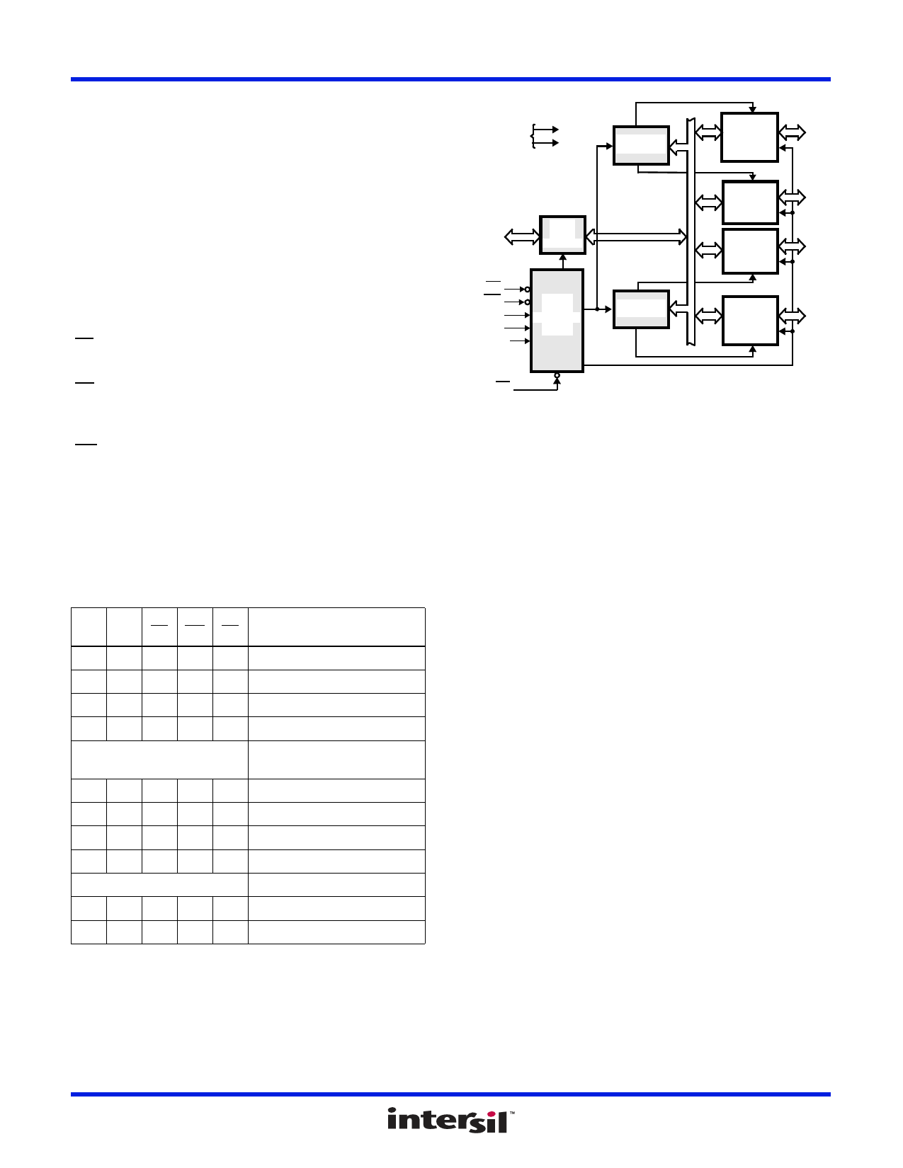
82C55A
Functional Description
Data Bus Buffer
This three-state bidirectional 8-bit buffer is used to interface the
82C55A to the system data bus. Data is transmitted or
received by the buffer upon execution of input or output
instructions by the CPU. Control words and status information
are also transferred through the data bus buffer.
Read/Write and Control Logic
The function of this block is to manage all of the internal and
external transfers of both Data and Control or Status words. It
accepts inputs from the CPU Address and Control busses and
in turn, issues commands to both of the Control Groups.
(CS) Chip Select. A “low” on this input pin enables the
communication between the 82C55A and the CPU.
(RD) Read. A “low” on this input pin enables 82C55A to send
the data or status information to the CPU on the data bus. In
essence, it allows the CPU to “read from” the 82C55A.
(WR) Write. A “low” on this input pin enables the CPU to write
data or control words into the 82C55A.
(A0 and A1) Port Select 0 and Port Select 1. These input
signals, in conjunction with the RD and WR inputs, control the
selection of one of the three ports or the control word register.
They are normally connected to the least significant bits of the
address bus (A0 and A1).
82C55A BASIC OPERATION
A1 A0 RD WR CS
INPUT OPERATION
(READ)
0 0 0 1 0 Port A Data Bus
0 1 0 1 0 Port B Data Bus
1 0 0 1 0 Port C Data Bus
1 1 0 1 0 Control Word Data Bus
OUTPUT OPERATION
(WRITE)
0 0 1 0 0 Data Bus Port A
0 1 1 0 0 Data Bus Port B
1 0 1 0 0 Data Bus Port C
1 1 1 0 0 Data Bus Control
DISABLE FUNCTION
X X X X 1 Data Bus Three-State
X X 1 1 0 Data Bus Three-State
(RESET) Reset. A “high” on this input initializes the control
register to 9Bh and all ports (A, B, C) are set to the input mode.
“Bus hold” devices internal to the 82C55A will hold the I/O port
inputs to a logic “1” state with a maximum hold current of
400A.
POWER
SUPPLIES
+5V
GND
GROUP A
CONTROL
BIDIRECTIONAL
DATA BUS
D7-D0
DATA
BUS
BUFFER
RD
WR
A1
A0
RESET
READ
WRITE
CONTROL
LOGIC
8-BIT
INTERNAL
DATA BUS
GROUP B
CONTROL
GROUP A
PORT A
(8)
GROUP A
PORT C
UPPER
(4)
GROUP B
PORT C
LOWER
(4)
GROUP B
PORT B
(8)
I/O
PA7-
PA0
I/O
PC7-
PC4
I/O
PC3-
PC0
I/O
PB7-
PB0
CS
FIGURE 1. 82C55A BLOCK DIAGRAM. DATA BUS BUFFER,
READ/WRITE, GROUP A & B CONTROL LOGIC
FUNCTIONS
Group A and Group B Controls
The functional configuration of each port is programmed by the
systems software. In essence, the CPU “outputs” a control
word to the 82C55A. The control word contains information
such as “mode”, “bit set”, “bit reset”, etc., that initializes the
functional configuration of the 82C55A.
Each of the Control blocks (Group A and Group B) accepts
“commands” from the Read/Write Control logic, receives
“control words” from the internal data bus and issues the
proper commands to its associated ports.
Control Group A - Port A and Port C upper (C7 - C4)
Control Group B - Port B and Port C lower (C3 - C0)
The control word register can be both written and read as
shown in the “Basic Operation” table. Figure 4 shows the
control word format for both Read and Write operations. When
the control word is read, bit D7 will always be a logic “1”, as this
implies control word mode information.
Ports A, B, and C
The 82C55A contains three 8-bit ports (A, B, and C). All can be
configured to a wide variety of functional characteristics by the
system software but each has its own special features or
“personality” to further enhance the power and flexibility of the
82C55A.
Port A One 8-bit data output latch/buffer and one 8-bit data
input latch. Both “pull-up” and “pull-down” bus-hold devices are
present on Port A. See Figure 2A.
Port B One 8-bit data input/output latch/buffer and one 8-bit
data input buffer. See Figure 2B.
Port C One 8-bit data output latch/buffer and one 8-bit data
input buffer (no latch for input). This port can be divided into
FN2969 Rev 11.00
Dec 8, 2015
Page 4 of 30
Share Link: 