IMIC9835 Ver la hoja de datos (PDF) - Cypress Semiconductor
Número de pieza
componentes Descripción
Lista de partido
IMIC9835
Cypress Semiconductor

IMIC9835 Datasheet PDF : 18 Pages
| |||
C9835
Table 4. Group Timing Relationships and Tolerances (continued)
CPU to SDRAM/DCLK
CPU to 3V66
Offset(ns)
3.75
0
CPU = 66.6 MHz, SDRAM = 100 MHz
CPU = 133.3MHz, SDRAM = 133.3MHz
Tolerance(ps)
Conditions
500
180 degrees phase shift
500
SDRAM/DCLK to 3V66
3V66 to PCI
PCI to IOAPIC
48M (0,1)
3.75
1.5–3.5
0
Async
500
500
1000
N/A
3V66 leads
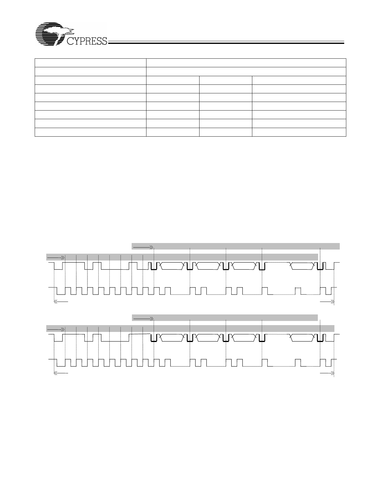
2-Wire SMBUS Control Interface
The 2-wire control interface implements a read/write slave
only interface according to SMBus specification. (SeeFigure 5
below). The device can be read back by using standard
SMBUS command bytes. Sub addressing is not supported,
thus all preceding bytes must be sent in order to change one
of the control bytes. The 2-wire control interface allows each
clock output to be individually enabled or disabled. 100 Kbits/s
(standard mode) data transfer is supported.
During normal data transfer, the SDATA signal only changes
when the SCLK signal is low, and is stable when SCLK is high.
There are two exceptions to this. A high to low transition on
SDATA while SCLK is high is used to indicate the start of a data
transfer cycle. A low to high transition on SDATA while SCLK
is high indicates the end of a data transfer cycle. Data is
always sent as complete 8-bit bytes, after which an
acknowledge is generated. The first byte of a transfer cycle is
an 8-bit address. The LSB address Byte = 0 in write mode.
The device will respond to transfers of 10 bytes (max) of data.
The device will generate an acknowledge (low) signal on
SDATA following reception of each byte. Data is transferred
MSB first at a max rate of 100kbits/s. This device will also
respond to a D3 address which sets it in a read mode. It will
not respond to any other control interface conditions, and
previously set control registers are retained.
When a clock driver is placed in power down mode, the
SMBUS signals SDATA and SCLK must be tri-stated. In power
down, the device retains all SMBUS programming information.
Transmit ACK
ACK
ACK
ACK
Receive 1 1 0 1 0 0 1 0 COMMAND BYTE
BYTE COUNT
BYTE 0
DATA
(Don’t Care)
(Don’t Care)
(Valid)
MSB
LSB
ACK
BYTE N
(Valid)
CLK
START CONDITION
8
8
8
Figure 5a (WRITE Cycle)
8
STOP CONDITION
Transmit ACK BYTE COUNT
BYTE 0
Receiv 1 1 0 1 0 0 1 1
DATA
MSB
LSB
(Valid)
ACK
(Valid)
BYTE1
ACK
ACK
(Valid)
BYTE N
ACK
(Valid)
CLK
START CONDITION
8
8
8
Figure 5b (READ Cycle)
Figure 5. SMBus Communications Waveforms
8
STOP CONDITION
Document #: 38-07303 Rev. **
Page 7 of 18
Share Link: