SMS44S Ver la hoja de datos (PDF) - Summit Microelectronics
Número de pieza
componentes Descripción
Lista de partido
SMS44S Datasheet PDF : 16 Pages
| |||
SMS44
PIN DESCRIPTIONS
V0 through V3
These inputs are used as the voltage monitor inputs and as
the voltage supply for the SMS44. Internally they are diode
ORed and the input with the highest voltage potential will
be the default supply voltage.
The RESET# output will be true if any one of the four inputs
is above 1V. However, for full device operation at least one
of the inputs must be at 2.7V or higher.
The sensing threshold for each input is independently
programmable in 20mV increments from 0.9V to 6.0V.
Also, the occurrence of an under- or over-voltage condi-
tion that is detected as a result of the threshold setting can
be used to generate subsequent action(s), such as RE-
SET# or IRQ#. The programmable nature of the threshold
voltage eliminates the need for external voltage divider
networks.
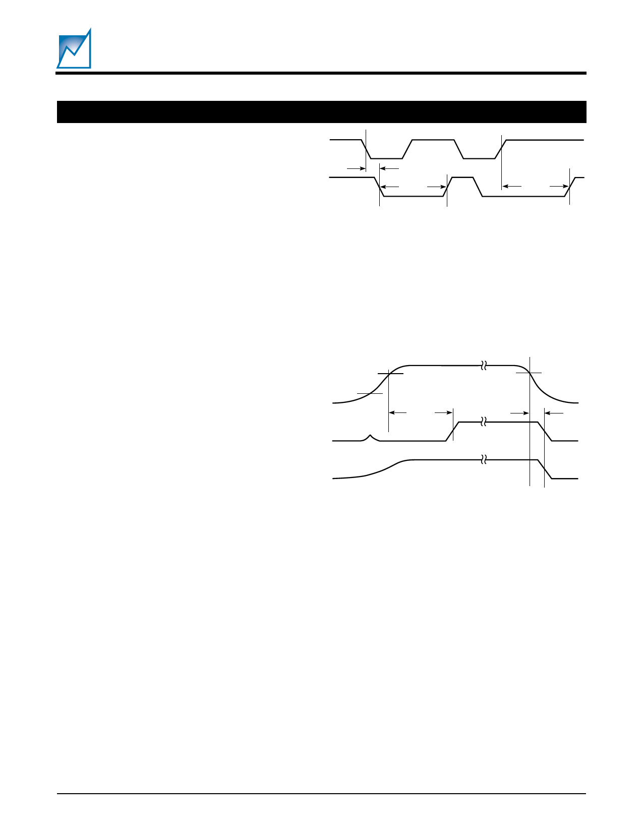
MR#
RESET#
tDMRRST
tPRTO
tPRTO
2047 Fig01 1.0
Figure 1. RESET# Timing with MR#
IRQ#
The interrupt output is an active low open-drain output. It
will be driven low whenever the watchdog timer times out
or whenever an enabled under-voltage or over-voltage
condition on a V input exists (configuration register 6).
PUP#1, PUP#2, PUP#3
These are the power-up permitted outputs when the
SMS44 is programmed to provide the sequencing of LDOs
or DC to DC converters. Each delay is independently
enabled and programmable for its duration (configura-
tion register 7). If all PUP# outputs are enabled the
sequence would be as follows: V0 above threshold then
delay to PUP#1 turning on; V1 above threshold then delay
to PUP#2 turning on; V2 above threshold then delay to
PUP#3 turning on to end the sequence.
V0 — V3
RESET#
IRQ#
VPTH
tPRTO
VRST
tD
MR#
The manual reset input always generates a RESET#
output whenever it is driven low. The duration of the
RESET# output pulse will be initiated when MR# goes low
and it will stay low for the duration of MR# low plus the
programmed reset timeout period (tPRTO). If MR# is
brought low during a power-on-sequence of the PUP#s the
sequence will be halted for the reset duration, and will then
resume from the point at which it was interrupted. If MR#
is low the configuration registers can be read or written to
so long as at least one of the VX inputs is ≥2.7V.
RESET#
The reset output is an active low open drain output. It will
be driven low whenever the MR# input is low or whenever
an enabled under-voltage or over-voltage condition exists,
or when a longdog timer expiration exists. The four voltage
monitor inputs are always functioning, but their ability to
generate a reset is programmable (configuration regis-
ter 4). Refer to figures 1 and 2 for a detailed illustration of
the relationship between MR#, IRQ#, RESET# and the VIN
levels.
2047 Fig02 1.1
Figure 2. RESET# Timing with IRQ#
WLDI
Watchdog and longdog timer interrupt input. A low to high
transition on the WLDI input will clear both the watchdog
and longdog timers, effectively starting a new timeout
period.
If WLDI is stuck low and no low-to-high transition is
received within the programmed tPWDTO period (pro-
grammed watch dog timeout) IRQ# will be driven low. If a
transition is still not received within the programmed
tPLDTO period (programmed longdog timeout) RESET# will
be driven low. Refer to Figure 3 for a detailed illustration.
Holding WLDI high will block interrupts from occurring but
will not block the longdog from timing out and generating
a reset. Refer to Figure 4 for a detailed illustration of the
relationship between IRQ#, RESET#, and WLDI.
SUMMIT MICROELECTRONICS, Inc.
2047 2.3 10/23/00
5
Share Link: 