LF4415 Ver la hoja de datos (PDF) - LUXPIA
Número de pieza
componentes Descripción
Lista de partido
LF4415 Datasheet PDF : 32 Pages
| |||
PRELIMINARY
LF4460
LF4430
LF4415
Video Memory / FIFO
Memory
Organization
Addressing
Flexibility
Simple
Configuration
& Control
LF4430 Overview
FRAME
MEMORY
Imagine a full-frame HDTV frame buffer solution in a single, tiny chip. Add a simple, easy to use SRAM
interface and complex addressing capability on-chip - and you have a LOGIC Devices HD Frame Memory.
The LF44xx Video Memory family supports all SDTV/HDTV video formats and range from 15 to 60Mbit
densities with configurable memory organizations and parallel word-widths. Independent (asynchronous)
clock domains on the device’s data I/O ports enable synchronization and rate matching. Since reads are
non-destructive, a given data value written into the memory core may be read as many times as desired.
Applications requiring additional depth may cascade devices for depth expansion.
In addition to memory organization flexibility, the LF44xx family simplifies memory addressing tasks. Timing
reference signals (TRS) on an incoming video signal can be detected and used to provide an auto-clear on
the Write pointer/address for simplified frame-sync applications. Write or Read pointers can be forced (in
real-time) to any location within the entire address space using an external 24bit address port. Full-time
Write or Read address manipulation using the external address port enables such applications as image
rotation, Region-of-Interest extraction, or Picture-in-Picture (PIP).
Devices are configured by simply tying off static control pins. If a more complex memory implementation
is required, access to application specific functions/features are provided through 8bit configuration words
programmed via a standard I2C serial interface.
MODE control pins define memory organization, I/O word width, and number of unique FIFO channels.
Combinations of MODE settings range from 8 to 24bit I/O in single or dual FIFO configurations.
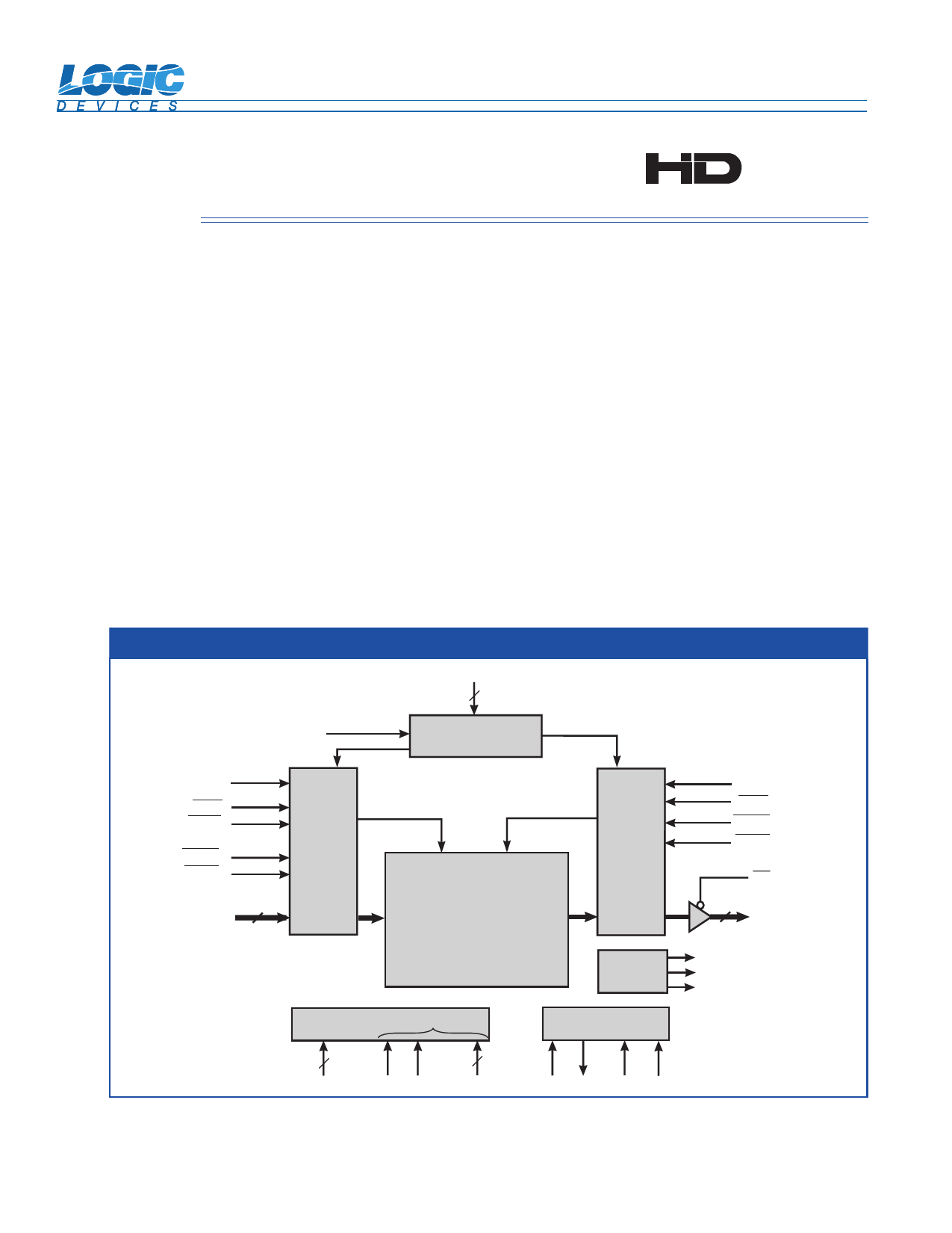
LF44xx Functional Block Diagram
ADDR[23:0]
24
RDWRB
ADDRESS OVERRIDE
CONTROL
WCLK
WEN
WIEN
WCLR
WSET
WRITE
ADDRESS
& CONTROL
READ
ADDRESS
& CONTROL
WRITE
CONTROL
MEMORY ARRAY
READ
CONTROL
24
D[23:0]
60 Mbit (LF4460)
30 Mbit (LF4430)
15 Mbit (LF4415)
FLAGS
RCLK
REN
RCLR
RSET
OE
24
Q[23:0]
PF0
COLLIDE0
PE0
MODE
I2C
JTAG
4
MODE
7
SDA SCL CHIP_ADDR6-0 TDI TDO TMS TCK
LOGIC Devices Incorporated
www.logicdevices.com
2
High Performance Memory Product
January 23, 2008 LDS-44xx-A
Share Link: 