BTS129 Ver la hoja de datos (PDF) - Siemens AG
Número de pieza
componentes Descripción
Lista de partido
BTS129 Datasheet PDF : 8 Pages
| |||
BTS 129
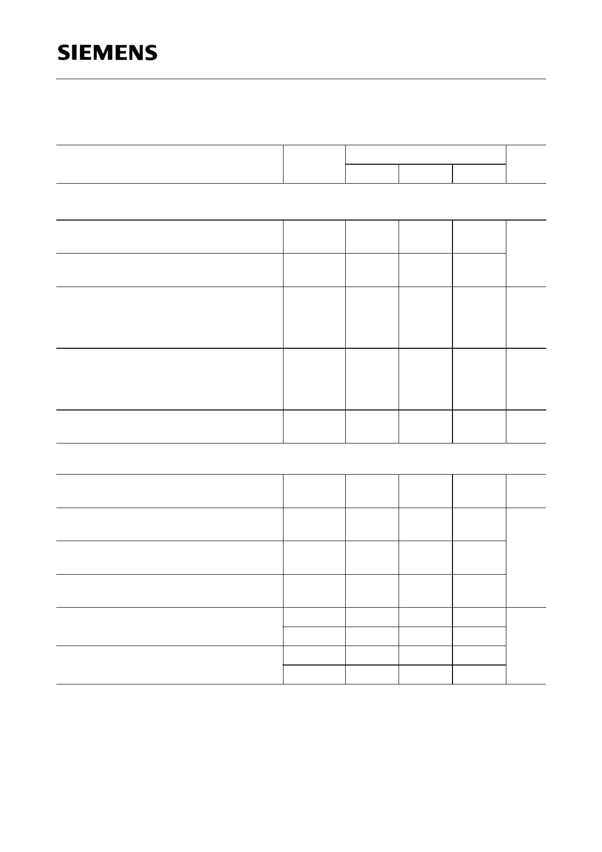
Electrical Characteristics
at Tj = 25 °C, unless otherwise specified.
Parameter
Symbol
min.
Static Characteristics
Drain-source breakdown voltage
VGS = 0, ID = 0.25 mA
Gate threshold voltage
VGS = VDS, ID = 1 mA
Zero gate voltage drain current
VGS = 0 V, VDS = 60 V
Tj = 25 °C
Tj = 150 °C
Gate-source leakage current
VGS = 20 V, VDS = 0
Tj = 25 °C
Tj = 150 °C
Drain-source on-state resistance
VGS = 10 V, ID =17 A
V(BR)DSS
60
VGS(th)
2.5
I DSS
–
–
I GSS
–
–
RDS(on)
–
Dynamic Characteristics
Forward transconductance
VDS ≥ 2 × ID × R , DS(on)max ID = 17 A
gfs
8.0
Input capacitance
VGS = 0, VDS = 25 V, f = 1 MHz
Ciss
700
Output capacitance
VGS = 0, VDS = 25 V, f = 1 MHz
Coss
–
Reverse transfer capacitance
VGS = 0, VDS = 25 V, f = 1 MHz
Crss
–
Turn-on time ton, (ton = td(on) + tr)
td(on)
–
VCC = 30 V, VGS = 10 V, ID = 3 A, RGS = 50 Ω tr
–
Turn-off time toff, (toff = td(off) + tf)
td(off)
–
VCC = 30 V, VGS = 10 V, ID = 3 A, RGS = 50 Ω tf
–
Values
Unit
typ.
max.
V
–
–
3.0
3.5
µA
1
10
100
300
10
100
nA
2
4
µA
Ω
0.04
0.05
S
13.0
18.0
pF
940
1250
500
750
180
270
25
40
ns
60
90
100
130
75
95
Semiconductor Group
2
Share Link: 