RF2483PCBA-41X(V2) Ver la hoja de datos (PDF) - RF Micro Devices
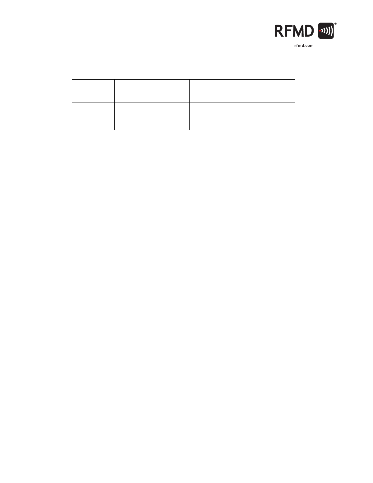
Número de pieza
componentes Descripción
Lista de partido
RF2483PCBA-41X Datasheet PDF : 28 Pages
| |||
RF2483
Pin Function Description
1
VCC3
Supply for RF output circuits.
Interface Schematic
VCC3
RF Output
Amplifier
2
VCC2
Supply for modulator and biasing circuits.
VCC2
Modulator and
VGA
VCC2
3
ISIG P
In phase I channel positive baseband input port. Best performance is
achieved when the ISIGP and ISIGN are driven differentially. The recom-
mended CW differential drive level (VISIGP-VISIGN) is 800mVP-P.
This input should be DC-biased at 1.2V±0.05V. The common-mode DC
coltage on the ISIGP and ISIGN input signals is used to bias the modulator.
In sleep mode an internal FET switch is opened, the input goes high imped-
ance and the modulator is de-biased. The input impedance is typically
5.5kΩ at low frequencies and at higher frequencies can be modeled as
V CC2
50Ω in series with 12pF to ground.
Phase or amplitude errors between the ISIGP and ISIGN signals may result
50 Ω
in the even order distortion of the modulation in the output spectrum.
DC offsets between the ISIGP and ISIGN signals will result in increased car-
rier leakage. Small DC offsets may be deliberately applied between the
12 pF
ISIGP/ISIGN and QSIGP/QSIGN inputs to cancel out LO leakage. The opti-
mum corrective DC offsets will change with mode, frequency and gain con-
trol.
Common-mode noise on the ISIGP and ISGN should be kept low as it may
degrade the noise performance of the modulator.
Phase offsets may be applied between the I and Q channels to improve the
sideband suppression performance.
4
ISIG N
In phase I channel negative baseband input port. See ISIGP.
V CC2
50 Ω
12 pF
5
ENABLE Enables power to the device.
CMOS input.
Logic 1 (1.4V to VCC)=Enabled.
Logic 0 (0V to 0.5V)=Powered Down.
V CC2
6
VCC1
Supply for the LO buffers and quadrature network.
The sideband suppression is a function of the VCC1 voltage. The inclusion VCC1
of R3 (39Ω) lowers the voltage on VCC1 by around 400mV and results an
improvement in sideband suppression but around a 0.2dB increase in
LO Quadrature
Generator and
noise at 20MHz offset.
Buffers
GND1
8 of 28
7628 Thorndike Road, Greensboro, NC 27409-9421 · For sales or technical
support, contact RFMD at (+1) 336-678-5570 or sales-support@rfmd.com.
Rev A8 DS060203
Share Link: 