MT9125AE Ver la hoja de datos (PDF) - Zarlink Semiconductor Inc
Número de pieza
componentes Descripción
Lista de partido
MT9125AE Datasheet PDF : 18 Pages
| |||
MT9125
Preliminary Information
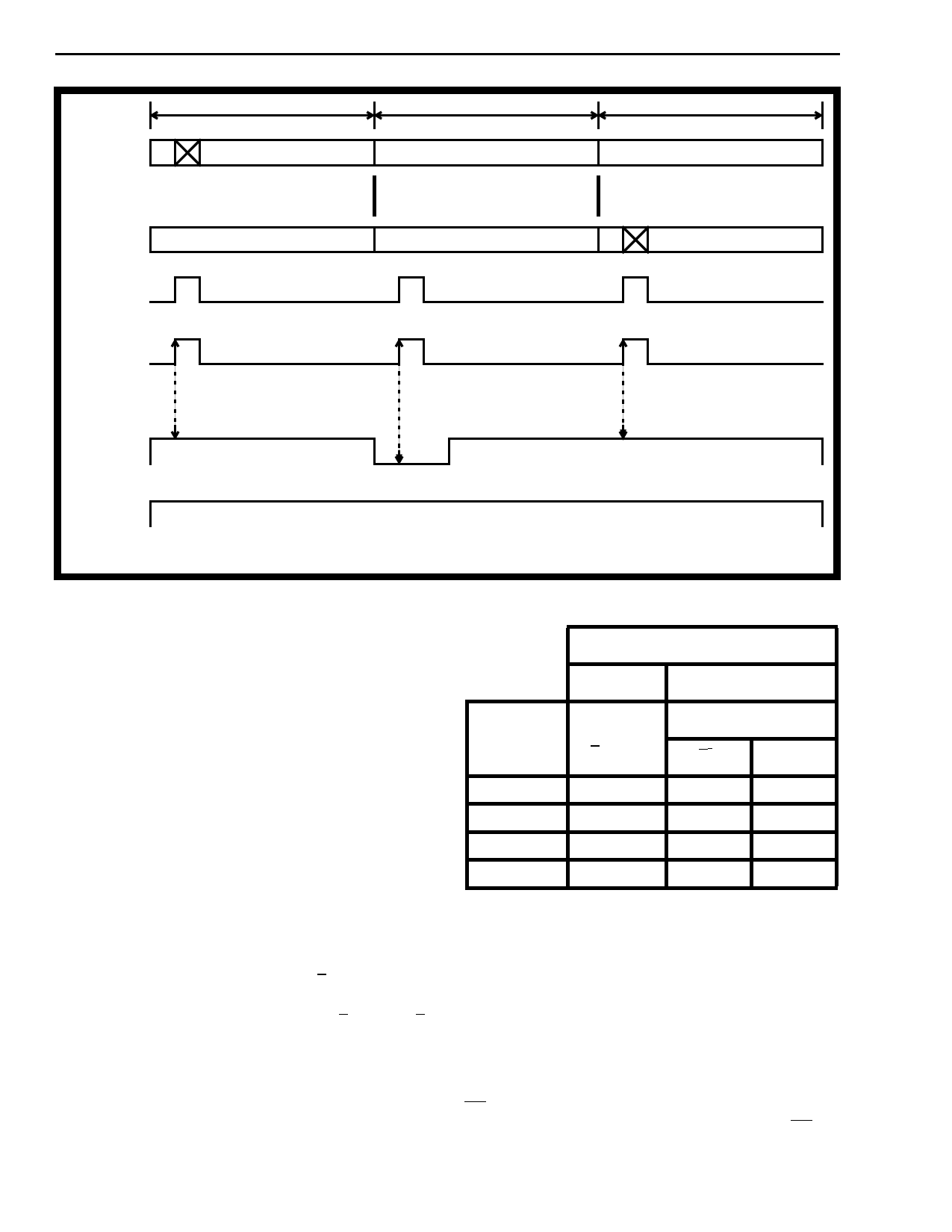
DSTi
ADPCMo
frame n-1
frame n
PCM Byte "X" latched into device
during frame n-1
PCM Byte "X" processed according
to MSn input states latched during
frame n
frame n+1
ADPCM Word "X" output from
device during frame n+1
ENA
ENB1 or
EN1
MS1/3
1,1=32 kb/s
1,0=24 kb/s
1,1=32 kb/s
MS2/4
This diagram shows the conversion sequence from PCM to ADPCM. The same pipelining occurs in the
reverse ADPCM to PCM direction.
Total delay from data input to data output = 2 frames. See Figure 15 for detailed ENB1/EN1 timing.
Figure 6 - Pipelining for Dynamic 32/24 kb/s Operation
Bit Clock (BCLK)
For SSI operation the bit rate, for both ADPCM and
PCM ports, is determined by the clock input at
BCLK. BCLK must be eight periods in duration and
synchronous with the 8 kHz frame input at ENB1.
Data is sampled at DSTi and at ADPCMi concurrent
with the falling edge of BCLK. Data is available at
DSTo and ADPCMo concurrent with the rising edge
of BCLK. BCLK may be any rate between 128 kHz
and 2.048 MHz. Refer to Figures 12 and 13.
For ST-BUS operation BCLK is ignored and the bit
rate is internally set to 2.048 MHz.
PCM Law Control (A/µ, FORMAT)
The PCM companding/coding law invoked by the
transcoder is controlled via the A/µ and FORMAT
pins. CCITT G.711 companding curves, µ-Law and
A-Law, are determined by the A/µ pin (0=µ-
Law; 1=A-Law). Per sample, digital code assignment
can conform to CCITT G.711 (when FORMAT=1) or
to Sign-Magnitude coding (when FORMAT=0). Table
1 illustrates these choices.
FORMAT
0
1
Sign-
CCITT (G.711)
PCM Code Magnitude
A/µ = 0 or 1 (A/µ = 0) (A/µ = 1)
+ Full Scale
+ Zero
- Zero
- Full Scale
1111 1111
1000 0000
1000 0000
1111 1111
0000 0000
0111 1111
0111 1111
0000 0000
Table 1
1010 1010
1101 0101
0101 0101
0010 1010
Processing Delay through the Device
One 8 kHz frame is required for serial loading of the
input buffers, and one frame is required for
processing, for a total of two frame delays through
the device. All internal input/output PCM and
ADPCM shift registers are parallel loaded through
secondary buffers on an internal frame pulse. The
device derives its internal frame reference from the
F0i, ENB1 and ENB2 pins in the following manner. If
a valid ST-BUS frame pulse is present at the F0i pin
the transcoder will assume ST-BUS operation and
will use this input as the frame reference. In this
8-80
Share Link: 