FM25V01A Ver la hoja de datos (PDF) - Cypress Semiconductor
Número de pieza
componentes Descripción
Lista de partido
FM25V01A Datasheet PDF : 22 Pages
| |||
FM25V01A
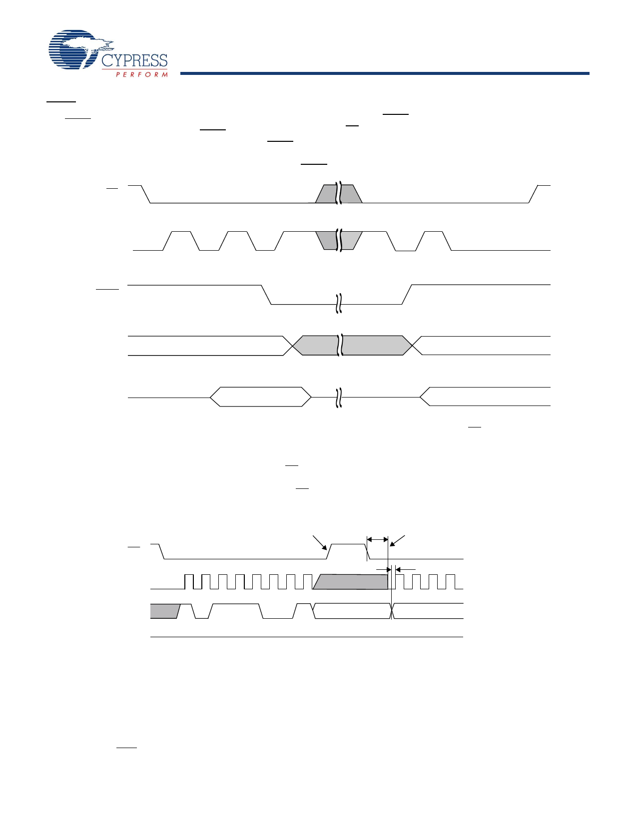
HOLD Pin Operation
The HOLD pin can be used to interrupt a serial operation without
aborting it. If the bus master pulls the HOLD pin LOW while SCK
is LOW, the current operation will pause. Taking the HOLD pin
HIGH while SCK is LOW will resume an operation. The
transitions of HOLD must occur while SCK is LOW, but the SCK
and CS pin can toggle during a hold state.
Figure 13. HOLD Operation [2]
CS
SCK
HOLD
SI
VALID IN
VALID IN
SO
Sleep Mode
A low-power sleep mode is implemented on the FM25V01A
device. The device will enter the low-power state when the
SLEEP opcode B9h is clocked-in and a rising edge of CS is
applied. When in sleep mode, the SCK and SI pins are ignored
and SO will be HI-Z, but the device continues to monitor the CS
pin. On the next falling edge of CS, the device will return to
normal operation within tREC time. The SO pin remains in a HI-Z
state during the wakeup period. The device does not necessarily
respond to an opcode within the wakeup period. To start the
wakeup procedure, the controller may send a “dummy” read, for
example, and wait the remaining tREC time.
Figure 14. Sleep Mode Operation
Enters Sleep Mode
tREC Recovers from Sleep Mode
CS
0123 456 7
t SU
SCK
SI
1011 1 00 1
SO
HI-Z
VALID IN
Note
2. Figure 13 shows HOLD operation for input mode and output mode.
Document Number: 001-90881 Rev. *E
Page 10 of 22
Share Link: 