2N5460 Ver la hoja de datos (PDF) - Vishay Semiconductors
Número de pieza
componentes Descripción
Lista de partido
2N5460 Datasheet PDF : 5 Pages
| |||
2N/SST5460 Series
Vishay Siliconix
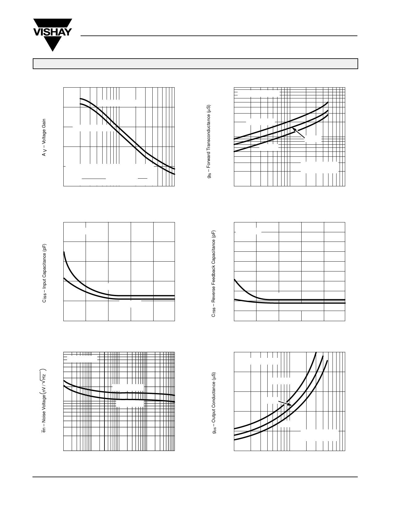
TYPICAL CHARACTERISTICS (TA = 25_C UNLESS OTHERWISE NOTED)
Circuit Voltage Gain vs. Drain Current
100
VGS(off) = 1.5 V
80
Common-Source Forward Transconductance
vs. Drain Current
10
VGS(off) = 3 V
60
VGS(off) = 3 V
40
TA = –55_C
1
125_C
25_C
20 Assume VDD = –15 V, VDS = –5 V
0
AV
+1
gfs RL
) RLgos
RL
+
10 V
ID
–0.01
–0.1
–1
ID – Drain Current (mA)
Common-Source Input Capacitance
vs. Gate-Source Voltage
10
f = 1 MHz
8
VDS = –15 V
f = 1 kHz
0.1
–0.1
–1
–10
ID – Drain Current (mA)
Common-Source Reverse Feedback Capacitance
vs. Gate-Source Voltage
5
f = 1 MHz
6
4
–5 V
2
–15 V
0
0
4
8
12
16
20
VGS – Gate-Source Voltage (V)
Equivalent Input Noise Voltage vs. Frequency
100
VDS = –15 V
ID = –0.1 mA
10
ID = –1 mA
1
10
100
1k
10 k
f – Frequency (Hz)
Document Number: 70262
S-04030—Rev. D, 04-Jun-01
100 k
2.5
–5 V
–15 V
0
0
4
8
12
16
20
VGS – Gate-Source Voltage (V)
Output Conductance vs. Drain Current
20
VGS(off) = 3 V
16
TA = –55_C
12
25_C
8
125_C
4
VDS = –15 V
f = 1 kHz
0
–0.1
–1
–10
ID – Drain Current (mA)
www.vishay.com
9-5
Share Link: 