IMIC9530CY Ver la hoja de datos (PDF) - Silicon Laboratories
Número de pieza
componentes Descripción
Lista de partido
IMIC9530CY Datasheet PDF : 10 Pages
| |||
C9530
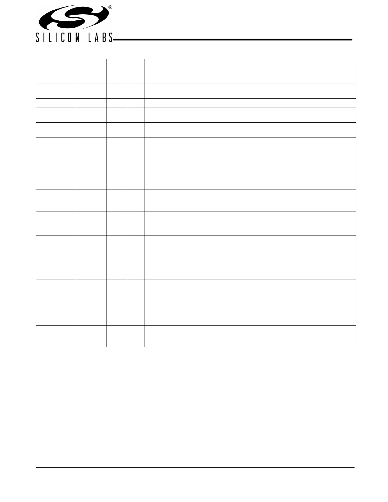
Pin Description[3]
Pin[2]
Name PWR[4] I/O
Description
3
XIN VDDA I Crystal Buffer input pin. Connects to a crystal, or an external clock source. Serves
as input clock TCLK, in Test mode.
4
XOUT VDDA O Crystal Buffer output pin. Connects to a crystal only. When a Can Oscillator is used
or in Test mode, this pin is kept unconnected.
1
REF VDD O Buffered inverted outputs of the signal applied at Xin, typically 33.33 or 25.0 MHz
24*
OEA VDD I Output Enable for clock bank A. Causes the CLKA output clocks to be in a
three-state condition when driven to a logic low level.
25*
OEB VDD I Output Enable for clock bank B. Causes the CLKB output clocks to be in a
three-state condition when driven to a logic low level.
18
AGOOD# VDD O When this output signal is a logic low level, it indicates that the output clocks of the
A bank are locked to the input reference clock. This output is latched.
31
BGOOD# VDD O When this output signal is at a logic low level, it indicates that the output clocks of
the B bank are locked to the input reference clock. This output is latched.
6*, 7*
SA(0,1) VDD
I Clock Bank A selection bits. These control the clock frequency that will be present
on the outputs of the A bank of buffers. See Table 1 for frequency codes and selection
values.
43*, 42*
SB(0,1) VDD
I Clock Bank B selection bits. These control the clock frequency that will be present
on the outputs of the B bank of buffers. See Table 1 for frequency codes and selection
values.
20*, 21*, 22* IA(0:2) VDD I SMBus address selection input pins. See Table 3 SMBus Address table.
27*
SSCG# VDD I Enables Spread Spectrum clock modulation when at a logic low level, see Spread
Spectrum Clocking on page 6.
48
SDATA VDD I/O Data for the internal SMBus circuitry.
47
SCLK VDD I Clock for the internal SMBus circuitry.
11, 14
VDDA
– PWR 3.3V common power supply pin for Bank A PCI clocks CLKA.
38, 35
VDDB
– PWR 3.3V common power supply pin for Bank B PCI clocks CLKB.
2, 44, 46
VDD
– PWR Power supply for internal Core logic.
23, 29, 30
AVDD
– PWR Power for internal analog circuitry. This supply should have a separately
decoupled current source from VDD.
9, 10, 12, 15, CLKA (0:4) VDDA O A bank of five XINx1, XINx2, XINx3 and XINx4 output clocks.
16
40, 39, 37, 34, CLKB (0:4) VDDB O A bank of five XINx1, XINx2, XINx3 and XINx4 output clocks.
33
5, 8, 13, 17,
19, 26, 28, 32,
36, 41, 45
VSS
– PWR Ground pins for the device.
Notes:
2. Pin numbers ending with * indicate that they contain device internal pull-up resistors that will insure that they are sensed as a logic 1 if no external circuitry is
connected to them.
3. A bypass capacitor (0.1 F) should be placed as close as possible to each VDD pin. If these bypass capacitors are not close to the pins their high-frequency
filtering characteristic will be cancelled by the lead inductance of the trace.
4. PWR = Power connection, I = Input, O = Output and I/O = both input and output functionality of the pin(s).
.......................Document #: 38-07033 Rev. *C Page 2 of 10
Share Link: 