IMIC9530CY Ver la hoja de datos (PDF) - Silicon Laboratories
Número de pieza
componentes Descripción
Lista de partido
IMIC9530CY Datasheet PDF : 10 Pages
| |||
C9530
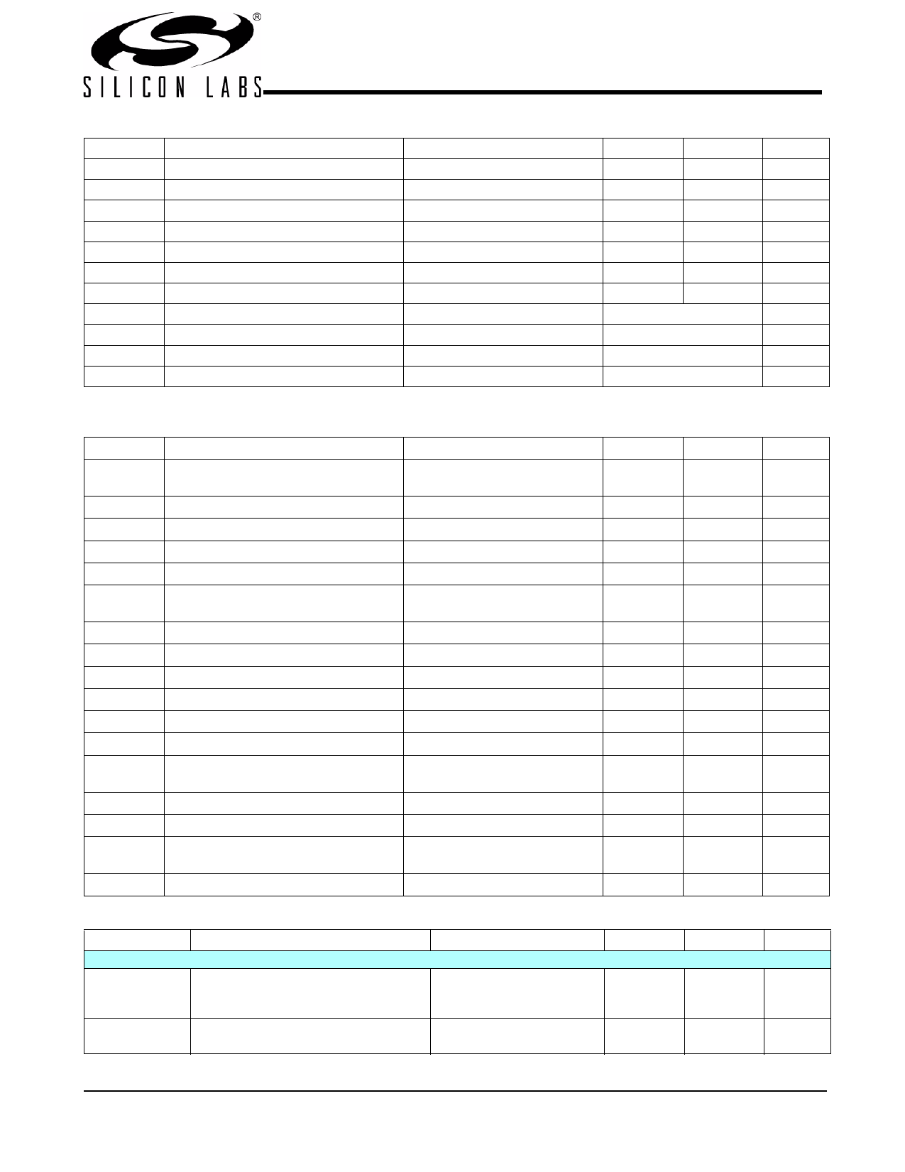
Absolute Maximum Conditions
Parameter
Description
Condition
Min.
Max.
VDD,VDDP
VDDA
VIN
TS
TA
TJ
ESDHBM
ØJC
ØJA
UL–94
Core Supply Voltage
Analog Supply Voltage
Input Voltage
Temperature, Storage
Temperature, Operating Ambient
Temperature, Junction
ESD Protection (Human Body Model)
Dissipation, Junction to Case
Dissipation, Junction to Ambient
Flammability Rating
Relative to V SS
Non Functional
Functional
Functional
MIL-STD-883, Method 3015
Mil-Spec 883E Method 1012.1
JEDEC (JESD 51)
At 1/8 in.
–0.5
4.6
–0.5
4.6
–0.5
–65
VDD + 0.5
+150
0
70
–
150
2000
–
15
45
V–0
MSL
Moisture Sensitivity Level
1
Multiple Supplies: The Voltage on any input or I/O pin cannot exceed the power pin during power-up. Power supply sequencing is NOT required.
DC Electrical Specifications
Parameter
Description
VDD, VDDA,
VDDB
VILI2C
VIHI2C
VIL
VIH
IIL
3.3 Operating Voltage
Input Low Voltage
Input High Voltage
Input Low Voltage
Input High Voltage
Input Leakage Current
VOL
VOH
IOZ
CIN
COUT
LIN
CXTAL
Output Low Voltage
Output High Voltage
High-Impedance Output Current
Input Pin Capacitance
Output Pin Capacitance
Pin Inductance
Crystal Pin Capacitance
VXIH
VXIL
IDD
Xin High Voltage
Xin Low Voltage
Dynamic Supply Current
IPD
Power-down Supply Current
Condition
3.3V ± 5%
SDATA, SCLK
SDATA, SCLK
S(A,B)O, S(A,B)1, OE(A,B)
except pull-ups or pull-downs
0 < VIN < VDD
IOL = 1 mA
IOH = –1 mA
From XIN and XOUT pins to
ground
At 133 MHz and all outputs
loaded per Table 8
PD# Asserted
Min.
3.135
Max.
3.465
–
2.2
VSS – 0.5
2.0
–5
1.0
–
0.8
VDD + 0. 5
5
–
0.4
2.4
–
–10
10
2
5
3
6
–
7
32
38
0.7VDD
0
–
VDD
0.3VDD
300
–
1
AC Electrical Specifications
Parameter
Crystal
TDC
Description
XIN Duty Cycle
XINFREQ
XIN Frequency
Condition
The device will operate
reliably with input duty cycles
up to 30/70%.
When Xin is driven from an
external clock source
Min.
45
25
Max.
55
33.3
Unit
V
V
VDC
°C
°C
°C
V
°C/W
°C/W
Unit
V
V
–
V
V
µA
V
V
µA
pF
pF
nH
pF
V
V
mA
mA
Unit
%
MHz
.......................Document #: 38-07033 Rev. *C Page 7 of 10
Share Link: 