ML7012-06 Ver la hoja de datos (PDF) - LAPIS Semiconductor Co., Ltd.
Número de pieza
componentes Descripción
Lista de partido
ML7012-06 Datasheet PDF : 23 Pages
| |||
FEDL7012-06-02
ML7012-06
Test Interface
Symbol
TST2 to 0
TI8 to 0
TO10 to 0
Type
Description
I Test pins for the LSI manufacturer. Input “0”.
In normal operation state, input “0” to all of the TI8 to 0.
The input combination in the table below realizes test modes. (Input “0” to TI8, TI6,
TI5, TI3, and TI2 in the case, too.)
TI7 TI4 TI1 TI0 Test function, description
1
0
0
0 Continuous output of DTMF tones (Code A)
1
1
0
0
Continuous output of originate scramble “1” of V.22bis
(2400bps)
I
1
1
0
1
Continuous output of answer scramble “1” of V.22bis
(2400bps)
AC loop test
1
0
1
0 It takes approx. 2 seconds to get into the AC loop test
mode. RTS signal is required to be ON.
When entering a test mode, execute reset using PDN/RST pin after TI8 to 0 are set as
intended.
When escaping from the test mode, execute reset using PDN/RST pin after TI8 to 0 are
set to “0”.
O Leave open
Power Supply
Symbol
VDDA
GNDA
VDD2 to 1
GND2 to 1
Type
I
I
I
I
Description
Analog VDD pin. Supply 2.7 - 3.6V.
Connect a ceramic capacitor with good high frequency characteristics (0.1 to 1µF) and an
electrolytic capacitor (10 to 20µF) in parallel between this terminal and GNDA.
Analog GND pin
Digital VDD pins. Supply 2.7 - 3.6V. Supply the same voltage to the VDDA.
Connect a ceramic capacitor with good high frequency characteristics (0.1 to 1µF) and an
electrolytic capacitor (10 to 20µF) in parallel between this terminal and GND2/GND1.
Digital GND pins.
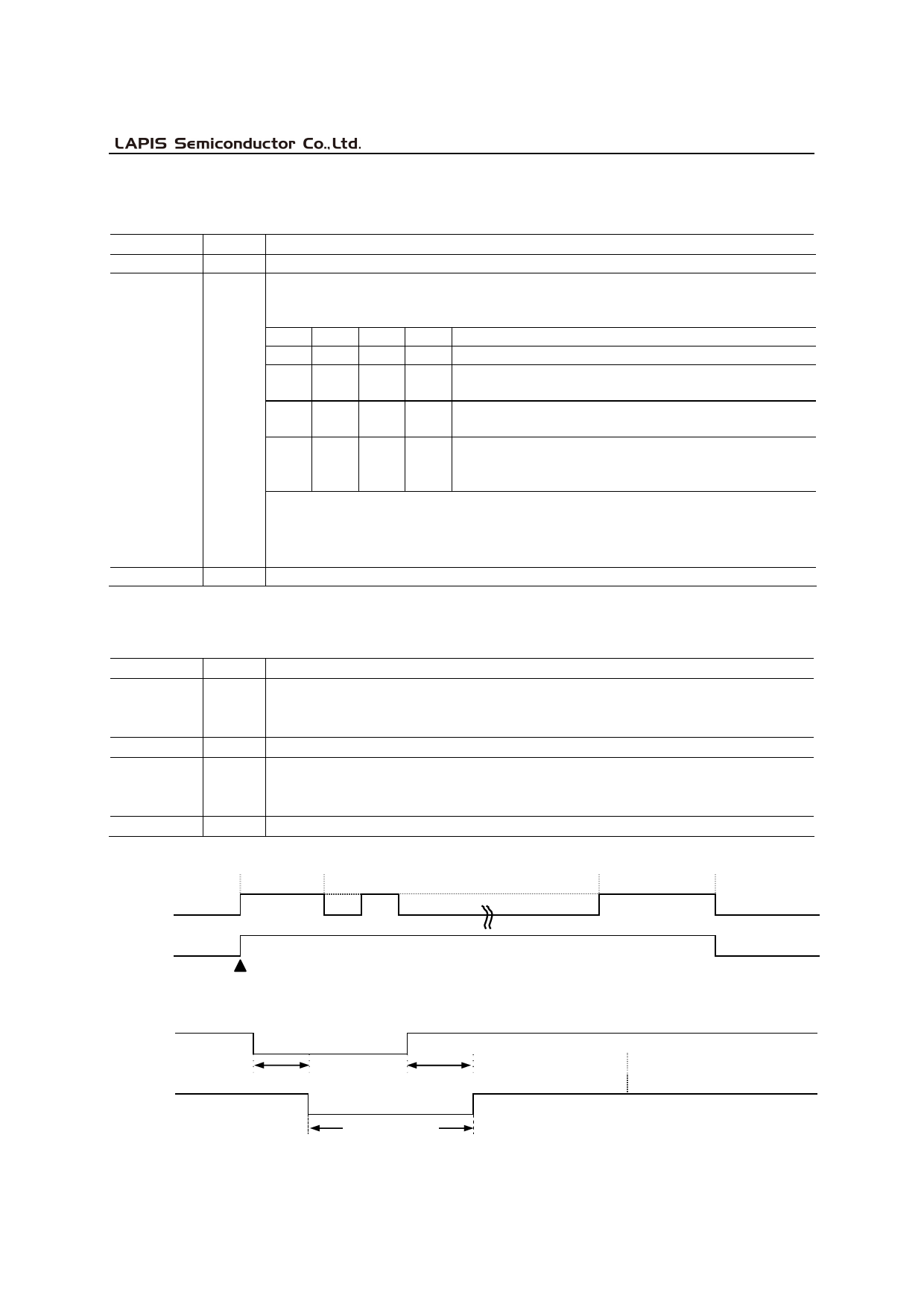
(*1)
RLY1
Pre-pause
Dialing
Communicating Commands
RLY2
(*2)
RII
CI
Line connection
150ms
400ms
a call-in signal
6/23
Share Link: 