AN246 Ver la hoja de datos (PDF) - STMicroelectronics
Número de pieza
componentes Descripción
Lista de partido
AN246 Datasheet PDF : 13 Pages
| |||
AN2466
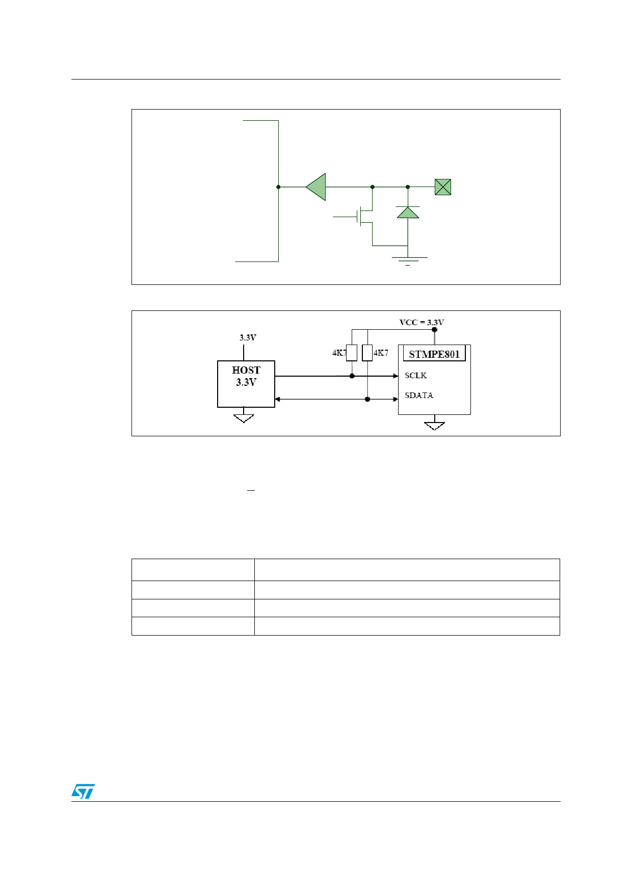
Figure 5. I2C pin structure
Pin description of STMPE801
INTERNAL
BLOCKS
INPUT BUFFER
Open
Drain
Buffer
PAD
ESD DIODE
Figure 6. I2C line with external pull-up resistors
2.2.1
I2C General call
STMPE801 supports I2C general call based on the following table. When a general call
address of 0x00 with R/ W = 0 is sent, the device responds with an acknowledgement and
performs the instruction given by the second byte. The device does not give ACK for any
second byte other than the valid second bytes listed in Table 3.
Table 3. I2C General call
Second byte
Definition
0x06
0x04
0x0
Slave device should reset and latch in the slave address
Slave device should latch in the slave address but without reset.
Not allowed as second byte.
2.3
Reset pin (RESET_N)
The Reset pin is an active low input. It should be tied HIGH to VIO supply in order to start
normal operation of the device. Apart from the RESET_N pin, the device can also be reset
through the "Soft_Reset" bit in the SYSCON register. Writing a '1' to Bit 7 resets the device
and after reset, the bit is cleared to '0' by the Hardware.
7/13
Share Link: 