AN246 Ver la hoja de datos (PDF) - STMicroelectronics
Número de pieza
componentes Descripción
Lista de partido
AN246 Datasheet PDF : 13 Pages
| |||
Pin description of STMPE801
AN2466
2.4
Interrupt pin (INT)
The interrupt pin is an open drain output pin with a structure similar to the SCL,SDA pins.
The INT output should be provided with a suitable pull-up resistor to VIO supply. The
interrupt output polarity can be configured as active low or active high by setting Bit 0 of the
SYSCON register. The interrupt output should be enabled by writing a '1' to Bit 2 in the
SYSCON. Even if individual GPIO interrupts are enabled, no interrupt will be generated if
the global INT_Enable bit is not set in the SYSCON. The Interrupt is cleared by reading the
ISGPIOR register (0x09). At reset, the interrupt output is disabled and the polarity is active
LOW.
Table 4.
Bit
7
6
5
4
3
2
1
0
SYSCON register
Reset
value
Name
Description
0
SoftReset Writing ‘1’ to this bit causes a soft reset of the device
0
I2C_SHDN
Writing ‘1’ to this bit shuts down the I2C block on the next
valid I2C clock.
0
0
0
0
INT_Enable ‘1’ to enable, ‘0’ to disable INT output
0
0
INTPolarity ‘1’ for active HI, ‘0’ for active LOW
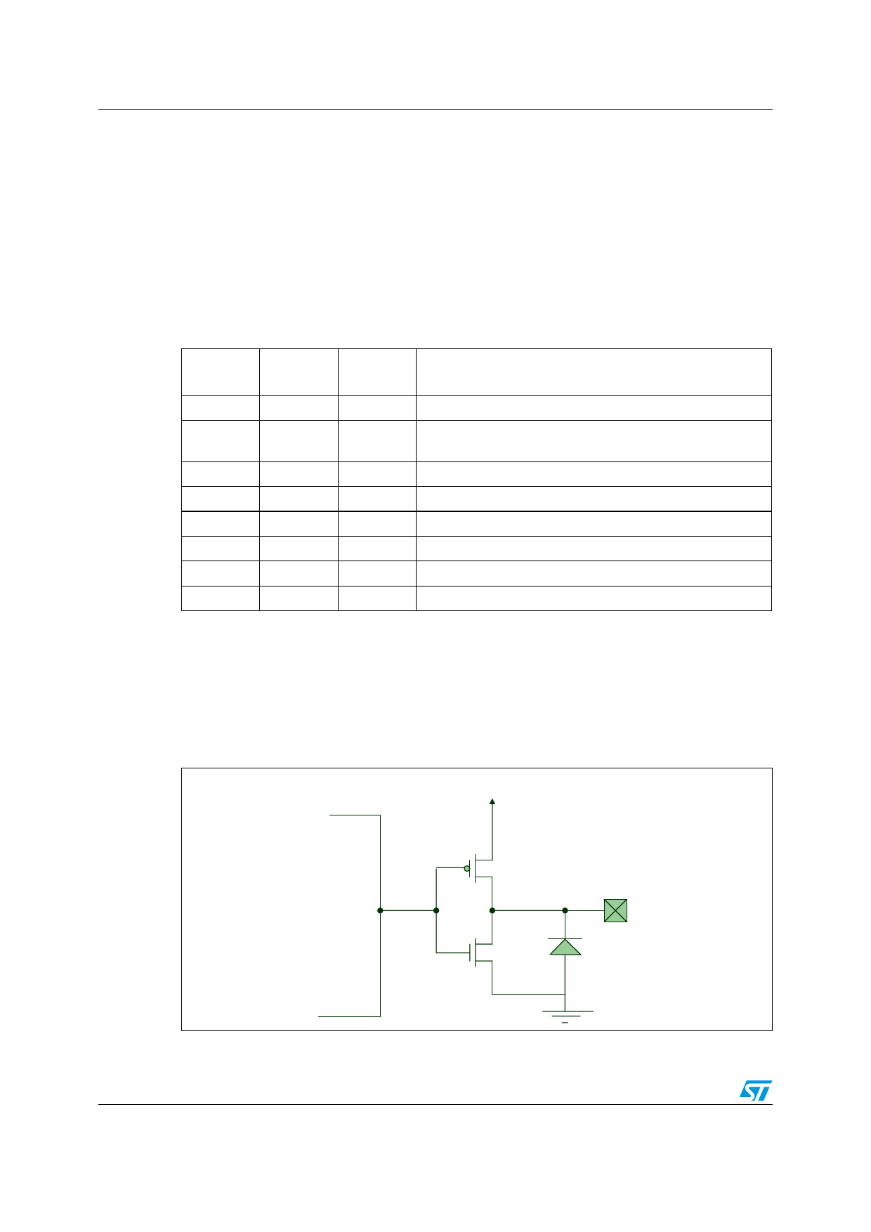
2.5
GPIO Pins
All 8 GPIO lines are configured as inputs at power-on/reset and are independent of each
other and can be individually programmed as input or output. Unused GPIOs should be
configured as outputs to minimize power consumption.
Figure 7. GPIO pin structure
VIO
P-BUFFER
INTERNAL
BLOCKS
N-BUFFER
PAD
ESD DIODE
8/13
Share Link: 