FAN5234 Ver la hoja de datos (PDF) - Fairchild Semiconductor
Número de pieza
componentes Descripción
Lista de partido
FAN5234 Datasheet PDF : 15 Pages
| |||
FAN5234
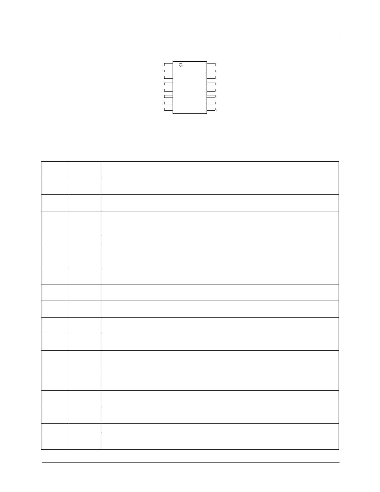
Pin Configurations
VIN
PGOOD
EN
ILIM
VOUT
VSEN
SS
AGND
1
16
2
15
3
14
4
13
FAN5234
5
12
6
11
7
10
8
9
FPWM
BOOT
HDRV
SW
ISNS
VCC
LDRV
PGND
QSOP-16 or TSSOP-16
θJA = 112°C/W
PRODUCT SPECIFICATION
Pin Definitions
Pin
Number Pin Name
1
VIN
2
PGOOD
3
EN
4
ILIM
5
VOUT
6
VSEN
7
SS
8
AGND
9
PGND
10
LDRV
11
VCC
12
ISNS
13
SW
14
HDRV
15
BOOT
16
FPWM
Pin Function Description
Input Voltage. Connect to main input power source (battery). Also used to program
operating frequency for low input voltage operation. See Table 1.
Power Good Flag. An open-drain output that will pull LOW when VSEN is outside of a
±10% range of the 0.9V reference.
ENABLE. Enables operation when pulled to logic high. Toggling EN will also reset the
regulator after a latched fault condition. This is a CMOS inputs whose state is
indeterminate if left open.
Current Limit. A resistor from this pin to GND sets the current limit.
Output Voltage. Connect to output voltage. Used for regulation to ensure a smooth
transitions during mode changes. When VOUT is expected to exceed VCC, tie this pin to
VCC.
Output Voltage Sense. The feedback from the output. Used for regulation as well as
PGOOD, under-voltage, and over-voltage protection and monitoring.
Soft Start. A capacitor from this pin to GND programs the slew rate of the converter
during initialization. During initialization, this pin is charged with a 5µA current source.
Analog Ground. This is the signal ground reference for the IC. All voltage levels are
measured with respect to this pin.
Power Ground. The return for the low-side MOSFET driver. Connect to source of low-
side MOSFET.
Low-Side Drive. The low-side (lower) MOSFET driver output. Connect to gate of low-side
MOSFET.
VCC. This pin powers the chip as well as the LDRV buffers. The IC starts to operate when
voltage on this pin exceeds 4.6V (UVLO rising) and shuts down when it drops below 4.3V
(UVLO falling).
Current Sense input. Monitors the voltage drop across the lower MOSFET or external
sense resistor for current feedback.
Switching node. Return for the high-side MOSFET driver and a current sense input.
Connect to source of high-side MOSFET and low-side MOSFET drain.
High-Side Drive. High-side (upper) MOSFET driver output. Connect to gate of high-side
MOSFET.
BOOT. Positive supply for the upper MOSFET driver. Connect as shown in Figure 2.
Forced PWM mode. When logic HIGH, inhibits the regulator from entering hysteretic
mode.
REV. 1.0.10 5/3/04
2
Share Link: 