CS5180-CL Ver la hoja de datos (PDF) - Cirrus Logic
Número de pieza
componentes Descripción
Lista de partido
CS5180-CL Datasheet PDF : 28 Pages
| |||
CS5180
SYNC pulse should rise on a falling edge of the
MCLK signal. This ensures that the SYNC input to
all CS5180s in the system will be recognized on the
next rising edge of MCLK. Use of the SYNC input
is not necessary to make the converter operate
properly. If it is unused it should be tied to DGND.
Conversion data is output from the SDO and SDO
pins of the device. The data is output from the SDO
pin MSB first, in two’s complement format. The
converter furnishes a serial clock SCLK and its
complement SCLK to latch the data bits; and a data
framing signal, Frame Sync Output (FSO), which
frames the output conversion word. The SCLK
output frequency is MCLK/3.
Clock Generator
The CS5180 must be driven from a CMOS-com-
patible clock at its MCLK pin. The MCLK input is
powered from the VD+ supply and its signal input
should not exceed this supply. The required
MCLK is 64 × OWR (Output Word Rate). To
achieve an Output Word Rate of 400 kHz, the
MCLK frequency must be 64 × 400 kHz, or
25.6 MHz. A second clock input pin, MCLK, is
not actually used inside the device but allows the
user to run a fully differential clock to the converter
to minimize radiated noise from the PC board lay-
out.
The CS5180 can be operated with MCLK frequen-
cies from 512 kHz up to 26 MHz. The output word
rate scales with the MCLK rate with
OWR = MCLK/64.
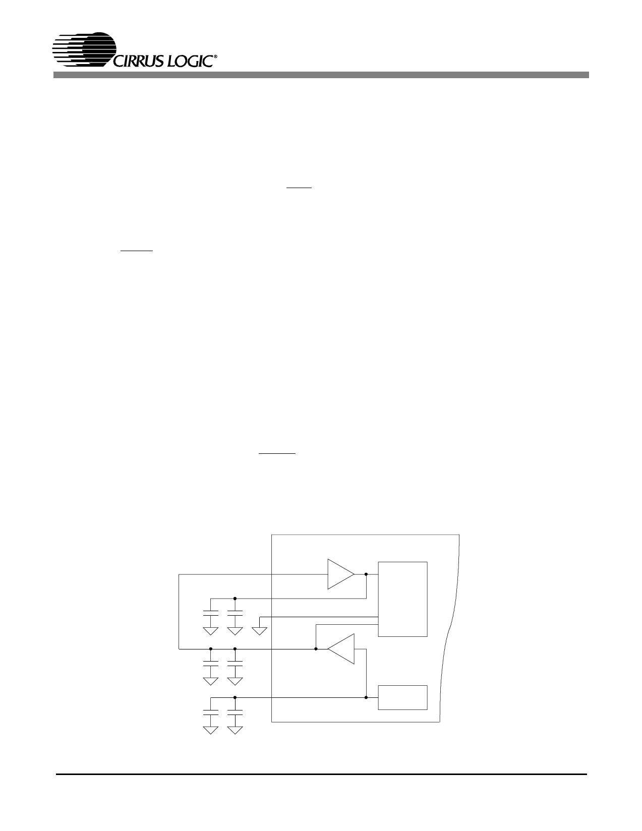
Voltage Reference
The CS5180 can be configured to operate from ei-
ther its internal voltage reference, or from an exter-
nal voltage reference.
The on-chip voltage reference is 2.375 V and is ref-
erenced to the AGND pin. This 2.375 V reference is
output from the VREFOUT pin. It is then filtered
and returned to the VREFIN pin. VREFIN pin is
connected to a buffer which has a gain of 1.6. This
scales the on-chip reference of 2.375 V to 3.8 V.
This value sets the peak-to-peak input voltage into
the AIN pins of the converter. Figure 3 illustrates the
CS5180 connected to use the internal voltage refer-
ence. Note that a 1.0 µF and 0.1 µF capacitor are
shown connected to the VREFCAP pin to filter out
noise. A larger capacitor can be used, but may re-
quire a longer reset period when first applying power
to the part to allow for the reference to charge up the
capacitors and stabilize before self-calibration be-
gins.
CS5180
10 µF +
VREFIN
0.1 µF
VREF+
VREF-
X1.6
Modulator
VREFOUT
X1
+
10 µF
0.1 µF
+
1 µF
VREFCAP
0.1 µF
Reference
Figure 3. CS5180 connection diagram for using the internal voltage reference.
10
Share Link: 