DM9102A Ver la hoja de datos (PDF) - Unspecified
Número de pieza
componentes Descripción
Lista de partido
DM9102A Datasheet PDF : 77 Pages
| |||
90
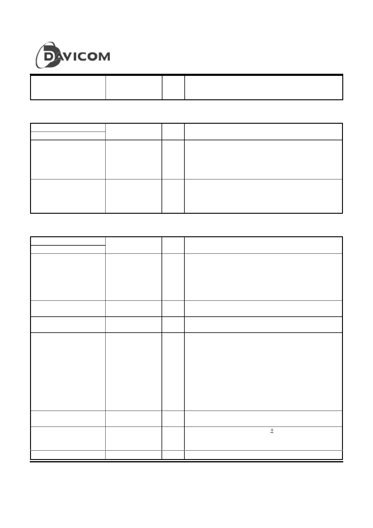
Network Interface
Pin No.
128QFP/128TQFP
105,106
109,110
SPEED10#
/ LINK#
DM9102A
Single Chip Fast Ethernet NIC controller
O LED output pin, active low
mode 0 = 10Mbps LED
mode 1 = Link LED
Pin Name
RXI+
RX-
TXO+
TXO-
I/O
Description
I 100M/10Mbps differential input pair.
These two pins are differential receive input pair for
100BASE-TX and 10BASE-T. They are capable of receiving
100BASE-TX MLT-3 or 10BASE-T Manchester encoded
data.
O 100M/10Mbps differential output pair.
These two pins are differential output pair for 100BASE-TX
and 10BASE-T. This output pair provides controlled rise and
fall times designed to filter the transmitter output.
Miscellaneous Pins
Pin No.
128QFP/128TQFP
36
71
75
95
97
98
102
12
Pin Name
I/O
Description
CLOCKRUN#
TEST2
TEST1
WOL/CSTSCHG
X2
X1/OSC
BGRES
I/O, Clockrun#
O/D The clockrun# signal is used by the system to pause or slow
down the PCI clock signal. It is used by the DM9102A to
enable or disable suspension of the PCI clock signal or restart
of the PCI clock. When the clockrun# signal is not used, this pin
should connected to an external pull-down resistor.
I TEST mode control 2
In normal operation, this pin is pulled-high.
I TEST mode control 1
In normal operation, this pin is pulled low.
O Wake up signal/Card Status Change
This is multiplexed pin to provide Wake on LAN signal or Card
Status Change. In a PCI system, it is used as a WOL signal. In
a CardBus system, it is used as the Card Status Change
output signal and is asynchronous to the clock signal. It
indicates that a power management event has occurred in a
CardBus system. The DM9102A can assert this pin if it detects
link status change, or magic packet, or sample frame. The
default is “normal low, active high pulse”. DM9102A also
support High/Low and Pulse/Level options.
O Crystal feedback output pin used for crystal connection only.
² Leave this pin open if oscillator is used.
I Crystal or Oscillator input. (25MHZ 50ppm)
25MHz Oscillator or series-resonance, fundamental
frequency crystal.
I Bandgap Voltage Reference Resistor.
Final
Version: DM9102A-DS-F03
August 28, 2000
Share Link: 