CB35000 Ver la hoja de datos (PDF) - STMicroelectronics
Número de pieza
componentes Descripción
Lista de partido
CB35000 Datasheet PDF : 16 Pages
| |||
CB35000 SERIES
LIBRARY OVERVIEW
The design of the CB35000 family has been
optimized to allow extremely high density, high
speed and low power designs. For these reasons
a wide range of cells with different ranges of
driving capability are available in the library.
The library cells have been optimized in term of
functional and electrical parameters in order to
have:
s Good balancing
s Maximum speed
s Optimum Threshold voltage
s Symmetric Vdd/Vss Noise margin
s Minimum Power-Speed figure
Surrounding the core are configurational
specialized transistors forming a Sea of I/O giving
a high degree of flexibility to the system designer.
The geometrical aspect of the cells was
configured to allow extremely dense design, fully
10 Êm
exploiting the features of the Place and Route
tool in terms of horizontal and vertical routing
grids. For Place and Route, three levels of metal
are utilized. Intracell and intercell wiring are
limited to first metal, with second and third metal
levels dedicated to interconnect wiring and power
distribution. Each cell gives the possibility to use
10 horizontal wiring channels using third metal.
With the horizontal grid unit being the same as
the Metal 2 minimum contacted pitch, the vertical
wiring can be done on every grid point, without
limitation.
TECHNOLOGY OVERVIEW
A major feature of the HCMOS5S process is
salicided active areas. This results in source
drain areas that are of one to two ohms
resistance as opposed to the hundreds or
thousands of ohms of source drain resistance in
previous technologies. This very low resistance is
one reason that very low transistor widths could
be utilized in the cell design since drive is not lost
due to source drain resistance. This use of low
width transistors results in lower capacitance
loading of the gates due to the smaller areas
utilized. Low resistance, low capacitance, and
small gates results in low power usage for
inverters as compared to previous technologies.
The reduction in power consumption allows the
usage of salicided active stripes to distribute
power internally to the simple cell, replacing, in
some cases, the usage of the first metal layer.
This saves silicon area by allowing greater
density, permeability and routability of the cells
resulting in greater overall circuit density.
The standard power distributions are Internal Vdd
and Vss, serving the internal cells and the
prebuffer sections of the I/O, External Vdd and
Vss serving the output transistors only, and
Receiver Vdd and Vss serving the first stages of
the receiver cells. Optional distributions for 5.0V
interface, GTL, CTL, and other standards can be
utilized as necessary.
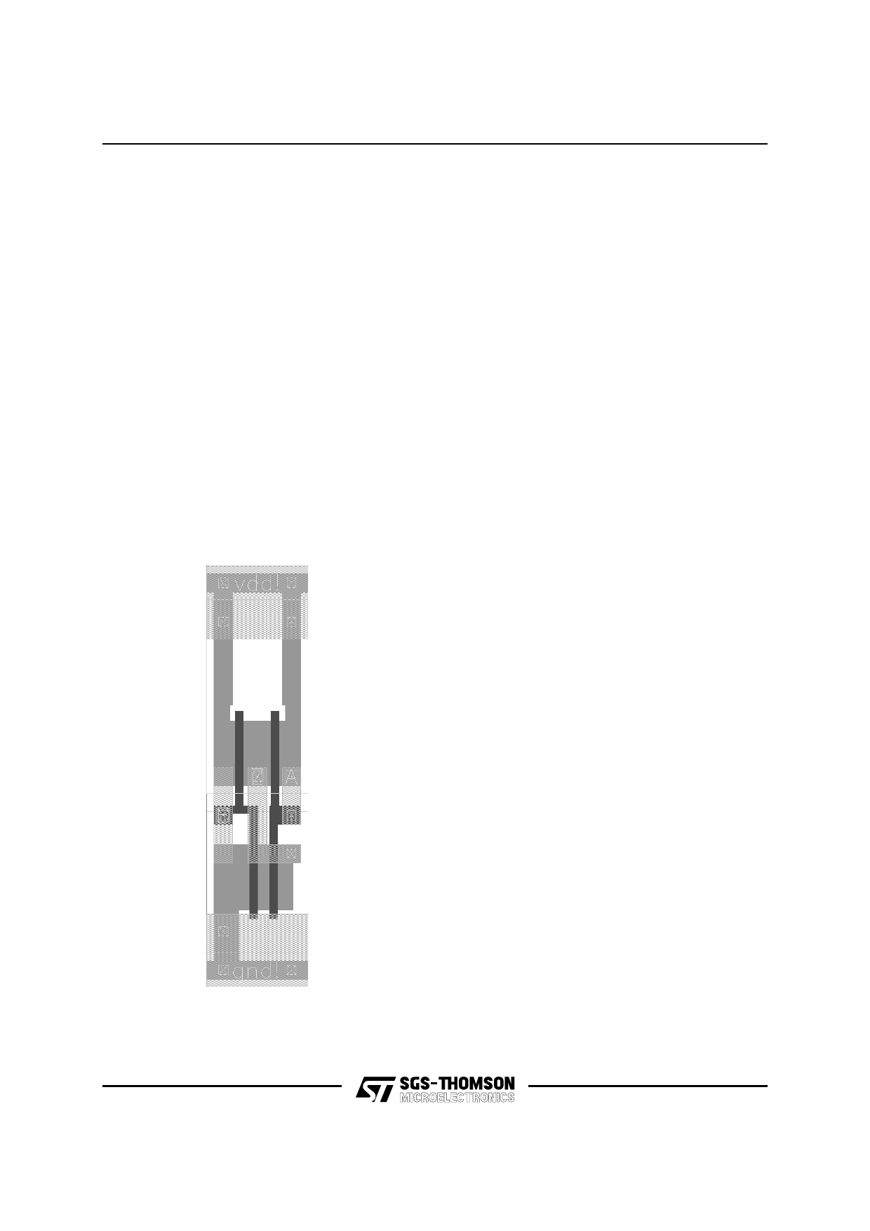
Figure 2. ND2 Core Cell
3/16
®
Share Link: 