MX98725 Ver la hoja de datos (PDF) - Macronix International
Número de pieza
componentes Descripción
Lista de partido
MX98725 Datasheet PDF : 33 Pages
| |||
MX98725
bit 24:Data parity Report, is set to 1 only if PERR# active and PFCS<6> is also set.
bit 26-25:Device Select Timing of DEVSELB pin.
bit 27:not used
bit 28:Receive Target Abort, is set to indicate a transaction is terminated by a target abort.
bit 29:Receive Master Abort, is set to indicate a master transaction with Master abort.
bit 30:Signal System Error, is set to indicate assertion of SERR#.
bit 31:Detected Parity Error, is set whenever a parity error detected regardless of PFCS<6>.
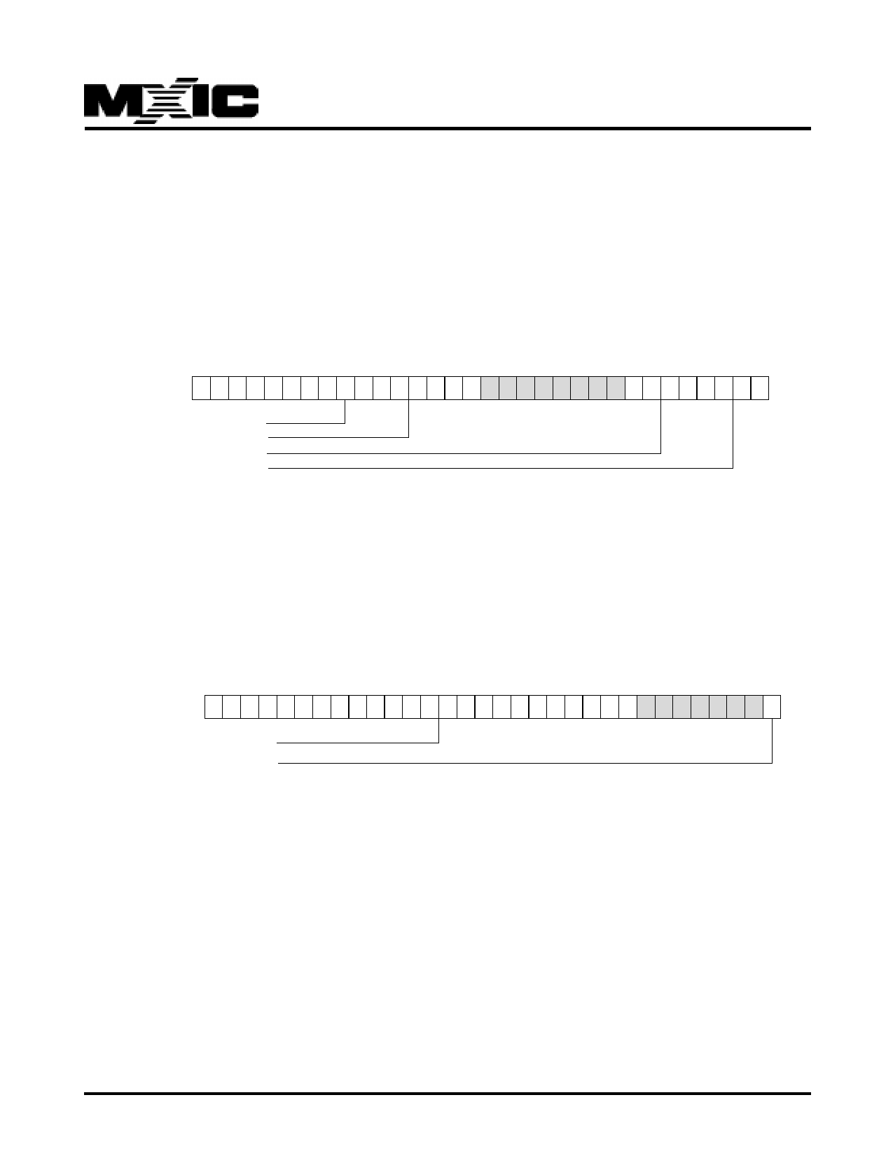
5.1.3 PCI REVISION REGISTER ( PFRV ) ( Offset 0Bh-08h )
31 30 29 28 27 26 25 24 23 22 21 20 19 18 17 16 15 14 13 12 11 10 9 8 7 6 5 4 3 2 1 0
Base Class
Subclass
Revision Number
Step Number
bit 3 - 0 : Step Number, range from 0 to Fh.
bit 7 - 4 : Revision Number, fixed to 3h for MX98725
bit 15 - 8 : not used
bit 23 - 16 : Subclass, fixed to 0h.
bit 31 - 24 : Base Class, fixed to 2h.
5.1.4 PCI BASE IO ADDRESS REGISTER ( PBIO ) ( Offset 13h-10h )
31 30 29 28 27 26 25 24 23 22 21 20 19 18 17 16 15 14 13 12 11 10 9 8 7 6 5 4 3 2 1 0
Configuration Base IO Address
IO/Memory Space Indicator
bit 0 : IO/Memory Space Indicator, fixed to 1 in this field will map into the IO space. This is a read only field.
bit 7 - 1 : not used, all 0 when read
bit 31 - 8 : Defines the address assignment mapping of MX98725 CSR registers.
P/N:PM0488
REV. 1.7, SEP. 15, 1998
7
Share Link: 