AD6426 Ver la hoja de datos (PDF) - Analog Devices
Número de pieza
componentes Descripción
Lista de partido
AD6426 Datasheet PDF : 50 Pages
| |||
Preliminary Technical Information
Wait
The H8 microprocessor WAIT input signal can be controlled
externally by programming the FLASHPWD pin to switch to
the WAIT input function. Setting the flag FLASHPWD Disable
in CC Control Register 77 to 1 and GPO11 Select to 0,
transforms the FLASHPWD output pin into a WAIT input pin.
External devices driving WAIT must drive high on reset and
until the software has changed the FLASHPWD pin to the
WAIT function.
Automatic Booting
To allow download of FLASH memory code into the final
system, the AD6426 provides a small dedicated routine to
transfer code through the Data Interface into the FLASH
memory. This routine is activated by asserting the
BOOTCODE pin.
Power Control
The AD6426 and Layer 1 software is optimized to minimize
the mobile radio power consumption in all modes of operation.
Two power control registers are dedicated for activating and
deactivating functional modules:
Bit POWER CONTROL INTERNAL CC Control
Register 44
2 Synthesizer Interface Power Enable
1 DSP Interface Power Enable
0 Encryption Power Enable
Bit POWER CONTROL EXTERNAL CC Control
Register 45
5 Output Clock Enable (will reset to 1)
4 General Purpose Power Control
2 DSP Power Control
1 Radio Power Control
INTERFACES
The GSM Processor provides eleven external interfaces for
dedicated purposes:
1. Memory Interface
2. EEPROM Interface
3. SIM Interface
4. Accessory Interface
5. Universal System Connector Interface
6. Keypad / Backlight / Display Interface
7. Battery ID Interface
8. Voiceband/Baseband Converter (EVBC)
Interface
9. Radio Interface
10. Test Interface
11. Debug Interface
AD6426
Memory Interface
The memory interface of the AD6426 serves two purposes.
Primarily, it provides the data, address, and control lines for
the external memories (RAM and ROM / FLASH Memory).
Secondly, the data and address lines are used to interface with
the display. The pins of the memory interface are listed in
Table 5.
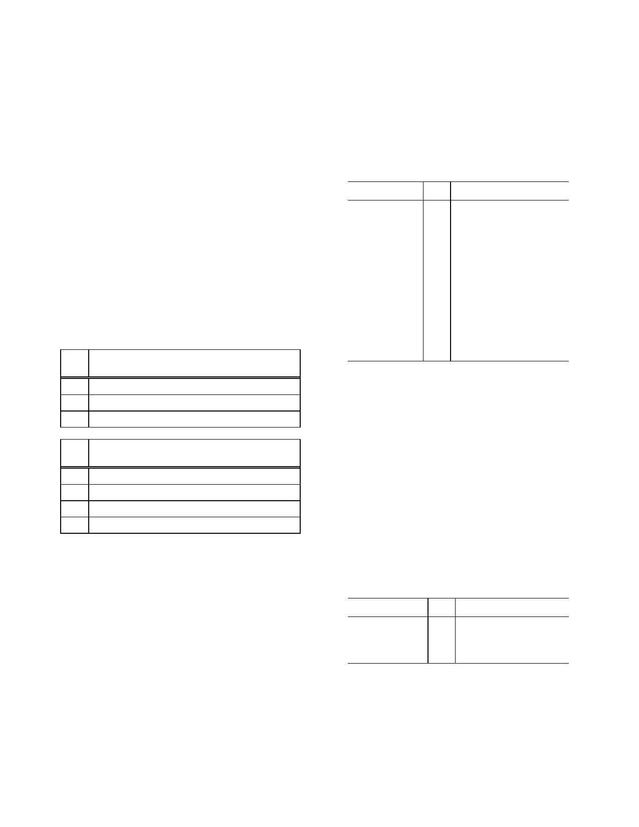
Table 5. Memory Interface
Name
ADD20 : 0
DATA15:0
RD
HWR
LWR
WR
RAMCS
ROMCS
FLASHPWD
I/O Function
O Address bus
I/O Data bus
O Read strobe
O High write strobe / Upper
Byte Strobe
O Low write strobe / Lower
Byte Strobe
O Write Strobe
O RAM chip select
O FLASH / ROM chip select
O FLASH Powerdown
The HWR and LWR pins can be configured to function as
UBS and LBS, respectively, by setting the SRAM16 bit (bit 0)
of the MEMIF H8 Peripheral Control Register 80. This bit is
reset at power-up. When configured as UBS and LBS, these
pins facilitate access of 16-bit SRAM in conjunction with the
Read/Write Strobes.
The pin FLASHPWD is automatically asserted low when the
H8 enters the Software Standby Mode, and de-asserted when
an interrupt causes the H8 to exit the Software Standby Mode.
This allows the use of “deep power down mode” for certain
FLASH memories. Also the entire data bus is driven low
during software standby mode.
EEPROM Interface
The AD6426 provides a 3-wire interface to an external
EEPROM by using three GPIOs of the control processor.
Table 6 shows the functionality of these three pins.
Table 6. EEPROM Interface
Name
EEPROMDATA
EEPROMCLK
EEPROMEN
I/O Function
I/O EEPROM data
O EEPROM clock
O EEPROM enable
This Information applies to a product under development. Its characteristics and specifications are subject to change without notice. Analog Devices assumes no
obligation regarding future manufacture unless otherwise agreed to in writing. No responsibility is assumed by Analog Devices for its use; nor for any
infringements of patents or other rights of third parties which may result from its use. No license is granted by implication or otherwise under any patent or patent
rights of Analog Devices.
Revision Preliminary 2.3 (June 9, ´98)
- 16 -
Confidential Information
Share Link: 