DM9102H Ver la hoja de datos (PDF) - Davicom Semiconductor, Inc.
Número de pieza
componentes Descripción
Lista de partido
DM9102H Datasheet PDF : 77 Pages
| |||
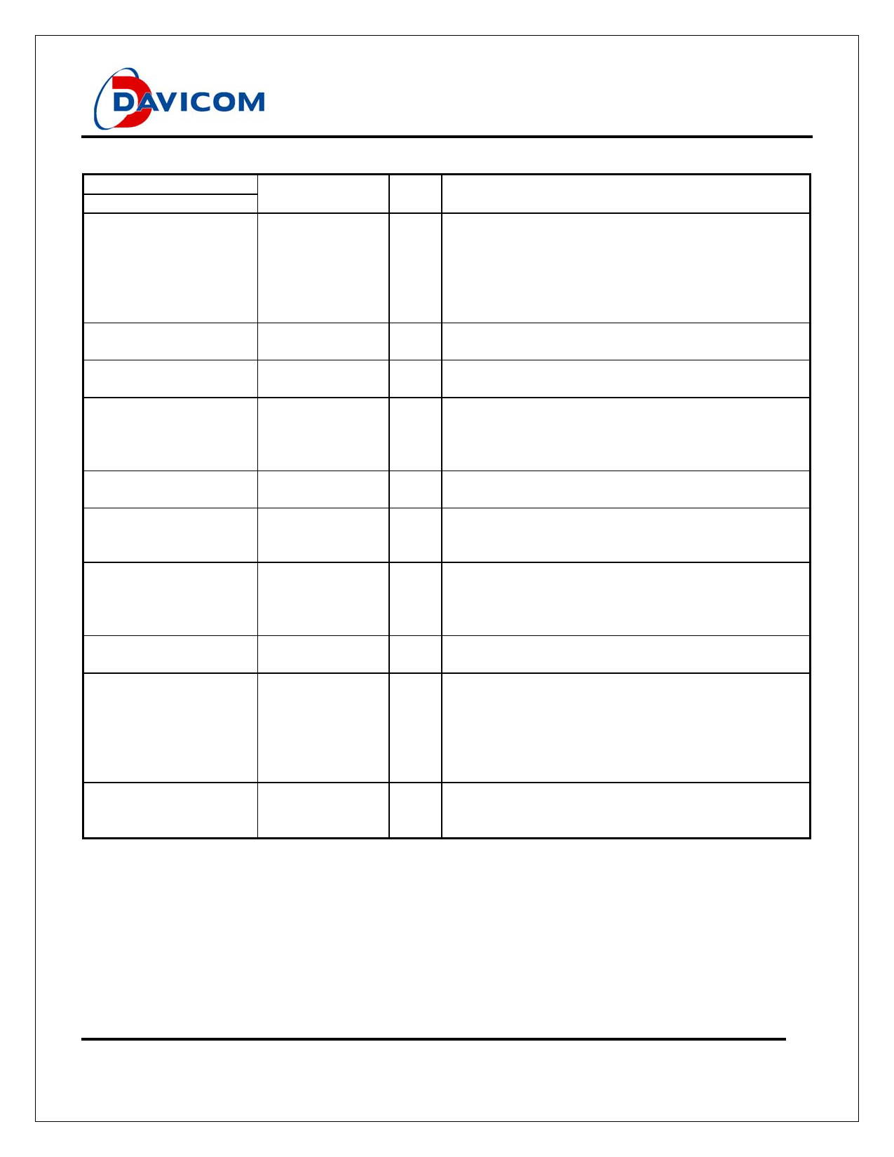
5.5 Miscellaneous Pins
Pin No.
128LQFP
36
71
37
94
97
98
102
101
116
95
Pin Name
CLOCKRUN#
TEST2
TEST1
WOL
X2
X1/OSC
BGRES
BGRESG
ISOLATE#
VCTRL18
DM9102H
Single Chip Fast Ethernet NIC Controller
I/O
Description
I/O, Clockrun#
O/D The clockrun# signal is used by the system to pause or slow
down the PCI clock signal. It is used by the DM9102H to
enable or disable suspension of the PCI clock signal or restart
of the PCI clock. When the clockrun# signal is not used, this pin
should be connected to an external pulled down resistor.
I TEST mode control 2
In normal operation, this pin is pulled high.
I TEST Mode Control 1
In normal operation, this pin is pulled low.
O Wake up signal. The DM9102H can assert this pin if it detects
link status change, magic packet, or sample frame. The default
is “normal low, active high pulse”. DM9102H also supports
High/Low and Pulse/Level options.
O Crystal feedback output pin is used for crystal connection only.
Leave this pin open if oscillator is used.
I Crystal or Oscillator Input. (25MHz±30ppm)
25MHz Oscillator or series resonance, fundamental
frequency crystal.
I Band gap Voltage Reference Resistor.
It connects to a 6.8KΩ1% error tolerance resistor between this
pin and BGRESG pin, to provide an accurate current reference
for DM9102H (10Base-T/100Base-TX Application).
I For Band gap Circuit
It is used together with the BGRES pin.
I Isolate
This isolate signal is used to isolate the DM9102H from the
system, and it is suitable for LAN on motherboard. When
isolate signal is active low, it disables the DM9102H function
and the DM9102H will not drive any outputs and sample any
inputs. In this case, the power consumption is minimum.
O Voltage 1.8V control
This pin can be used to control a BJT transistor‘s base pin to
generate a stable 1.8V power in BJT’s collect pin.
Final
6
Version: DM9102H-12-DS-F01
February 15, 2008
Share Link: 